


Ion Implantation Process Parameters
Jan 21, 2025
Leave a message
In silicon wafer fabrication, the distribution of ions plays a decisive role in device performance, which in turn is closely linked to the main parameters of the ion implantation process. The main parameters of ion implantation technology cover factors such as the type of ion source, injection dose, injection energy, injection angle, and rotation of the silicon wafer.
Ion implantation process parameters
1)Implantation Dose
The overall concentration of doped ions is mainly affected by the injected dose. The dose is determined by the product of the beam density (i.e., the number of ions per unit area) and the implantation time, and its specific range is closely related to the performance of the ion implantation device. Generally, the dose range of medium beam/high energy injection machine is 1011 ~1014cm-2. The high beam injector is between 1014~1016cm-2, and the theoretical formula for calculating the dose is:

0040-09094 CHAMBER 200mm
where N represents the ion implantation dose (unit: cm-19C). T is the injection time, I is the amount of the injected current; A is the injection area, n is the number of charges, and e is the unit charge.It is important to note that the ion implantation dose is measured in terms of beam density (i.e., the number of ions per unit area), whereas in actual concentration analysis, such as secondary ion mass spectrometry (SIMS), it is expressed in bulk concentration (i.e., the number of ions per unit volume). Therefore, when using these two methods, one should pay attention to the difference in their units of calculation.
Implantation Energy
The energy at the time of ion implantation, which is directly related to the speed of movement of the ions, is a key factor in determining the depth of ion implantation. In integrated circuit manufacturing, the energy range of ion implantation is typically between 0.1 keV and 1000 keV.
The depth of implantation of ions is not only related to the injection energy, but also to the injection dose. As shown in the figure below, the depth distribution of Sb ions under different energy injections is shown, which is obtained by SIMS analysis. It can be observed that as the injection energy increases, the depth of ion implantation also increases, but correspondingly, the peak concentration decreases.
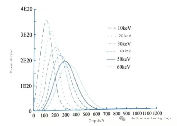
Depth distribution curves of Sb ions under different energy injections (SIME analysis)
The figure below depicts the curves of the injection depth of B, P, and As ions in amorphous silicon as a function of the injection energy. It is clear from the graph that there is a proportional relationship between the injection depth and the injection energy. In addition, for different kinds of ions with the same implantation energy, the greater the relative atomic mass of the ion, the smaller the projected range (Rp) of the implantation depth.
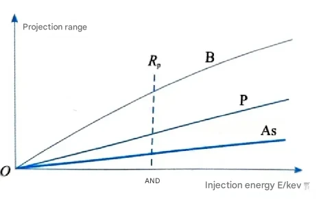
Curves of B, P, As injection depth in amorphous silicon as a function of injection energy
3)Implantation Angle
The angle parameters of ion implantation include tilt and twist, as shown in the figure below. The inclination angle has a significant impact on the ion implantation depth, while the twist angle needs to be adjusted accordingly according to the orientation of the specific product structure.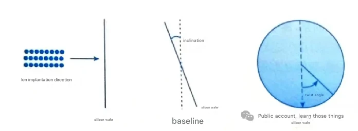
Inclination and twist angles of ion implantation
In the actual wafer process, silicon crystals exist as single crystals, exhibiting a specific crystal structure. Therefore, when viewed from different crystal directions, the lattice projection will show a large difference. As shown in the figure below, when viewed in the direction of <110 >, a large number of channels with large dimensions are formed. If you deviate from this angle, the number of channels increases, but the size decreases significantly. When ions are injected in the <110 > direction, some of the ions advance along these channels with minimal hindrance to the nuclei and electrons, resulting in a deeper than expected injection, resulting in a so-called channel effect.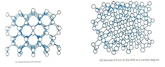
0020-33806 Upper Chamber Dps + Poly
Viewing Directions
Under the influence of the channel effect, there is a second peak in the depth and concentration of the ion implantation, as shown in the figure below, making the depth of the implantation difficult to control. In order to avoid the channel effect, two main methods are adopted: one is to adjust the main axis direction of the silicon crystal so that it deviates from the injection direction, that is, to adjust the inclination angle (usually between 3° and 7°) to make the silicon crystal appear amorphous. By observing the SIMS depth distribution curves of doped ions such as As, Sb, B, and P at different inclination angles (e.g., 5°, 30°, 60°, and 80°), it can be found that with the increase of inclination, the injection depth decreases, the peak value is closer to the surface, and the peak concentration decreases. The second is to cover the surface of the silicon crystal with an amorphous dielectric film, such as silicon dioxide and silicon nitride, or to amorphize the surface (such as implanting Ge or Si plasma).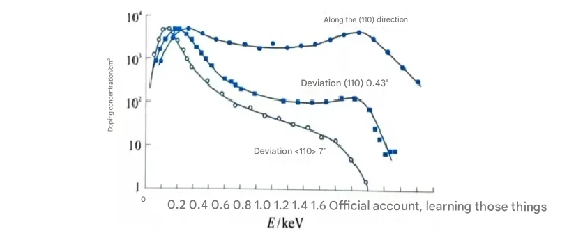 PEffect of channel effect on concentration distribution under 110 keV energy injection
4)Wafer Revolve
When ion implantation is carried out on silicon wafers, there is often a certain structural pattern on the surface, which causes parts of the area to be occluded during the injection process, resulting in the so-called shadow effect. In order to improve the injection uniformity of the silicon wafer surface, it is often necessary to rotate the silicon wafer. For example, in some ion implantation processes, the wafer is rotated four times at 90° for a quarter of the total dose to eliminate the effects of shading (see figure below, note: the dotted line is the shaded area).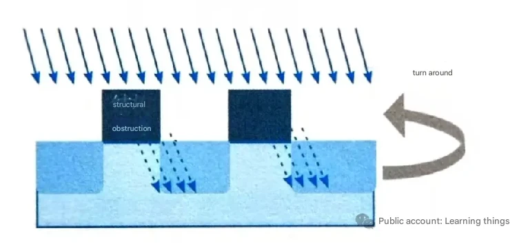
Ion inclination injection structure blocking
5)Selection of ion source There are many types of doping elements, including boron (B), phosphorus (P), arsenic (As), indium (In), oxygen (O), hydrogen (H), fluorine (F) and germanium (Ge). Depending on the application needs of the product, different elements need to be doped. The commonly used ion sources for boron are boron trifluoride (BF₃) or borane (B₂H₆), which are used for P-type doping, such as the formation of P-type traps, the adjustment of the threshold voltage of P-type devices, the doping of P-type devices, and the formation of source drains. Due to the low mass of boron atoms and the relatively low amount of implantation energy required, BF₃⁺ ions are usually selected for implantation.
Phosphorus is often used as an ion source for phosphine (PH₃) or solid red phosphorus for N-type doping, such as the formation of N-type traps, the adjustment of the threshold voltage of N-type devices, the doping of N-type devices, and the formation of source drains.
Arsenic can be used as an ion source, arsenic (AsH₃), solid arsenic or As₂O, which is N-type doped like phosphorus, and arsenic can also be used for injection in deep buried layers. Indium is indium iodide (InI) as the ion source, which is P-doped like boron, and is often used for light doping injection as a heavy ion.
Fluorine can be used as an ion source to neutralize the Si suspension key at the Si/SiO₂ interface to reduce the density of states at the interface and reduce the interference of leakage current and random electrical signal noise.
When injected with high doses, germanium can disrupt the lattice structure of silicon and form an amorphous layer, which helps to reduce the channel effect. In addition, it aids in recrystallization and electrical activation during annealing after ion implantation.
Monitoring of the ion implantation process
The parameters of the ion implantation process have a significant impact on the performance of the final product device, so it is important to monitor the process continuously and effectively. Here are a few main types of monitoring:
Thermal Wave Damage Detection Technology (see figure below)
After ion implantation, the crystal lattice of a silicon wafer will be damaged to a certain extent. By detecting the extent of this lattice damage, we can monitor the stability of the ion implantation process. This is done by heating the surface of the wafer with a laser beam, and then the reflectivity of the wafer surface changes. When a specific area of the wafer surface is measured with another laser, the reflected signal changes with the change in reflectivity, and this detected change is called a thermal wave (TW) signal. The thermal wave signal is closely related to the degree of damage to the crystal lattice. This method reacts quickly without wafer damage, making it ideal for real-time monitoring of the stability of the ion implantation process on the production line.
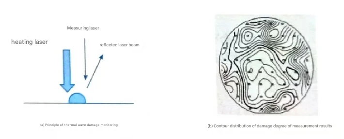 热波操作监控
2)Square resistance measurement The wafer after ion implantation needs to undergo rapid thermal annealing to stimulate the electronic activity of the dopants. The Sheet Resistance (RS) meter uses the four-probe method, in which an electric current is applied between two test pins and the voltage between the other two test pins is measured to calculate the square resistance value of the wafer. The RS value is a commonly used monitoring index in ion implanters, which is related to the injection dose and angle. In general, the higher the dose, the smaller the Rs value. The measurement results of Rs are also affected by the stability of the rapid thermal annealing process. Although this method is not as straightforward as thermal wave damage detection, its results are more accurate and are therefore widely used for in-line monitoring on production lines.
Secondary ion mass spectrometry By bombarding the wafer surface with a heavy ion beam and collecting the mass spectra of secondary ions sputtered at different times, we can measure the type, concentration, and depth of the doped elements. This is currently the most accurate monitoring method for ion implantation. However, SIMS analysis does not allow for a comprehensive analysis of the entire wafer, requires analysis in a dedicated laboratory using SIMS analysis equipment, and requires the destruction of the wafer for sampling, so in-line measurement is not possible, and the feedback time is relatively long.
4)Surface particle monitoring technology For ion implantation processes, the main hazard of surface particles is that they block the doped injection zone, resulting in incomplete doping structures, which in turn can affect the yield of the product. Therefore, we need to use methods such as electron microscopy to monitor surface particles.
Send Inquiry