


How Do Semiconductor Chips Work?
Oct 31, 2024
Leave a message
0020-42285 PLATE,BLOCKER 8" EC WXZ
0010-35756 CVD Cooldown Chamber Assy
█ Vacuum tube (electron tube)
The Edison Effect
In 1883, the famous inventor Thomas Edison observed a strange phenomenon during an experiment. At that time, he was conducting a life test of the filament (carbon filament). Next to the filament, he placed a copper wire, but the copper wire was not attached to any of the electrodes. That is, the copper wire is not energized .
.
After the carbon filament is energized normally, it begins to glow and heat. After a while, Edison disconnected the power supply. He accidentally discovered that an electric current had also been generated on the copper wire.
Edison had no way of explaining the reason for this phenomenon, but, as a shrewd "businessman", the first thing that came to his mind was to patent the discovery. He also named this phenomenon the "Edison effect".
Now we know that the essence of the "Edison effect" is the emission of thermal electrons. That is, when the filament is heated, the electrons on the surface become active and "escape", and as a result, they are captured by the metal copper wire, which generates an electric current.
When Edison applied for a patent, he didn't think about the use of the effect and put it on the shelf.
In 1884, the English physicist John Ambrose Fleming visited the United States to meet with Edison. Edison showed Fleming the Edison Effect and made a great impression on Fleming.
弗莱明
Diode
By the time Fleming actually used this effect, it was more than a decade later. In 1901, Guglielmo Marconi, the inventor of wireless telegraphy, launched experiments with long-range radio communication across the Atlantic. Fleming joined the experiment to help with how to enhance wireless signal reception. To put it simply, it is to study how to detect the signal at the receiving end and amplify the signal so that the signal can be perfectly interpreted.放大Everyone understands the signal, so what is a detection signal?
The so-called signal detection is actually signal screening. The signal received by the antenna is very messy, and there are all kinds of signals. The signals we really need (signals of a specified frequency) that need to be "filtered" out of these cluttered signals, and that is detection.
In order to achieve detection, unidirectional conductivity (unidirectional conductivity) is the key. Wireless magnetic waves are high-frequency oscillations, up to hundreds of thousands of times per second. The induced current generated by the wireless electromagnetic wave also changes with the "positive, negative, positive, negative", if we use this current to drive the earphone, one positive and one negative is zero, and the earphone will not be able to accurately identify the signal.
With unidirectional conductivity, the negative half-cycle of the sine wave is gone, all of them are positive, and the direction of the current is the same. By filtering out the high frequencies, the headphones can easily sense changes in current.
去掉负半周,电流方向变成一致的,容易解读
In order to detect the signal, Fleming thought of the "Edison effect" - could a new type of detector be designed based on the flow of electrons from the Edison effect? In this way, in 1904, the world's first vacuum electron diode was born under Fleming's hands. At the time, this diode was also called the "Fleming valve". (Vacuum tube, also known as electron tube, is sometimes called a "bile duct.") )
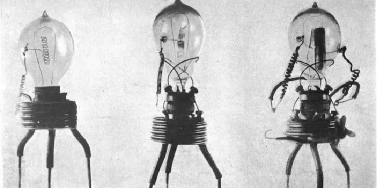
弗莱明发明的二极管
Fleming's diode, the structure is actually very simple, that is, in a vacuum glass bulb, two poles are stuffed: a cathode (cathode), which can emit electrons (cathode rays) when heated; An anode that receives electrons.
旁热式二极管
The reason why the vacuum in the glass tube is to prevent the ionization of gases, which will affect the normal flow of electrons and destroy the characteristic curve. (Pumping into a vacuum can also effectively reduce the oxidation loss of filament.) )
Transistor
The advent of diodes, which solved the need for detection and rectification, was a major breakthrough at that time. However, it has room for improvement.
德福雷斯特
In 1906, the American scientist De Forest Lee (De Forest Lee) invented the vacuum triode electron tube by cleverly adding a grid plate ("gate") to the vacuum diode electron tube.
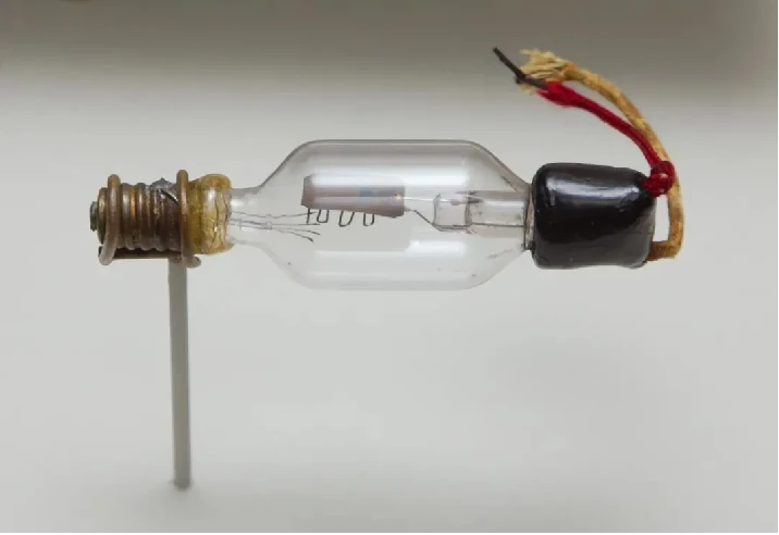
德·福雷斯特发明的三极管
When the gate is added, when the voltage of the gate is positive, it attracts more electrons from the cathode. Most of the electrons pass through the gate and reach the anode, which will greatly increase the current on the anode. If the voltage at the gate is negative, the electrons on the cathode have no power to go to the gate, let alone the anode.

A small change in current at the gate can cause a large change in current at the anode. Moreover, the changing waveform is exactly the same as the gate current. Therefore, the transistor has the effect of signal amplification.
At first, the triode was a single grid, then it became a double grid with two boards sandwiched together, and then it simply became a whole enclosed grid.
围栅
The birth of the vacuum triode is a milestone event in the field of electronics industry.
This small component truly realizes the use of electricity to control electricity (in the past, it was controlled by mechanical switches, which had the problems of low frequency, short life and easy damage), and used "small current" to control "large current".
This small component truly realizes the use of electricity to control electricity (in the past, it was controlled by mechanical switches, which had the problems of low frequency, short life and easy damage), and used "small current" to control "large current".
Based on it, we have radio stations, radios, phonographs, movies, radios, radars, radio intercoms, etc., which are becoming more and more powerful. The widespread popularity of these products has changed people's daily lives and promoted social progress.
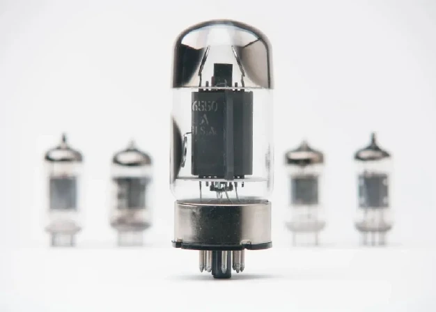
真空管
In 1919, Schottky of Germany proposed the idea of adding a curtain gate between the gate and the positive pole. This idea was realized by Lande in England in 1926. This became the quadrude. Later, Holst and Telegen of the Netherlands invented the pentode.
In the 40s of the 20th century, the research of computer technology entered a climax. It has been found that the unidirectional conductivity of electron tubes can be used to design some logic circuits (e.g., and gate circuits, or gate circuits).
So, they began to introduce electron tubes into the computer field. At that time, almost all electronic computers, including ENIAC (which used more than 18,000 tubes), were based on tubes.
埃尼阿克
Here we briefly talk about the gate circuit. When we learn the basics of computing, we must have learned basic logical operations, such as and, or, not, XOR, same or, NOT, or not, etc.

Computers only recognize 0s and 1s. It does its calculations based on these rules of logical operations. For example, 2+1 is 0010+0001 in binary, and doing "XOR operation" is equal to 0011, which is 3.
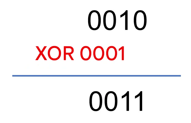
The circuit that implements the above logic gate functions is the logic gate circuit. On the other hand, a single-conductive electron tube (vacuum tube) can be assembled into various logic gate circuits. For example, "OR Gate" and "AND Gate" below.
 A, B are the inputs, and F are the output
█ transistors
At the same time of the rapid development and application of electron tubes, people have gradually found that there are some drawbacks in this product:
On the one hand, the tube is easy to break and has a high failure rate; On the other hand, the tube needs to be heated, and a lot of energy is wasted on heat generation, which also brings extremely high power consumption.
So, people started to think about whether there was a better way to detect, rectify, and amplify the signal. Of course, there are ways. At this time, a great material is about to appear, and it is - semiconductors.
The germ of semiconductors
Let's go back in time to the 18th century. In 1782, the famous Italian physicist Alessandro Volta (Alessandro Volta) found that solid matter can be roughly divided into three types:
The first, metals such as gold, silver, copper, iron, etc., are extremely conductive and are called conductors;
Second, materials like wood, glass, ceramics, mica, etc., which are not easy to conduct electricity, are called insulators;
The third, between a conductor and an insulator, discharges slowly.
The strange properties of the third material are named "Semiconducting Nature" by Volt, which means "semiconductor properties". This is the first time in human history that the term "semiconductor" has appeared.
亚历山德罗·伏特
Later, a number of scientists, intentionally or unintentionally, discovered some semiconductor properties. For example, in 1833, Michael Faraday discovered that when the temperature of silver sulfide increases, the resistance decreases (the heat-sensitive property of semiconductors).
In 1839, the French scientist Alexandre Edmond Becquerel discovered that light could cause a potential difference between the two ends of certain materials (the photovoltaic effect of semiconductors).
In 1873, Willoughby Smith discovered that the conductivity of selenium materials increases when exposed to light (the photoconductive effect of semiconductors).
These phenomena, no one was able to explain them at the time, and they did not attract much attention.
In 1874, the German scientist Karl Ferdinand Braun discovered the unidirectional conduction properties of electric current in natural ores (metal sulfides). This is a huge milestone.
卡尔·布劳恩
In 1906, the American engineer Greenleaf Whittier Pickard, based on the chalmer ore crystal, invented the famous crystal detector, also known as the "cat whisker detector" (the geophone has a probe on it, much like a cat's whisker, hence the name).
矿石检波器
The ore geophone is the earliest semiconductor device of mankind. Its appearance is a "small test" of semiconductor materials. Although it had some shortcomings (poor quality control, unstable work, because the ore was not of high purity), it gave a strong impetus to the development of electronic technology. At that time, radio receivers based on ore geophones promoted the popularization of broadcasting and wireless telegraphy.
The advent of the band theory
People use ore geophones, but they never understand how they work. In the more than 30 years since, scientists have repeatedly asked why there are semiconductor materials. Why can semiconductor materials be used for unidirectional conduction?
In the early days, many people even doubted that semiconductor materials really existed. The famous physicist Pauli once said, "People shouldn't be studying semiconductors, it's a dirty mess, and who knows if there are semiconductors." "
Later, with the birth and development of quantum mechanics, there was finally a breakthrough in the theoretical research of semiconductors.
In 1928, Max Karl Ernst Ludwig Planck, a German physicist and one of the founders of quantum mechanics, first proposed the theory of solid energy bands in the application of quantum mechanics to study the conduction of metals.
量子理论之父,普朗克
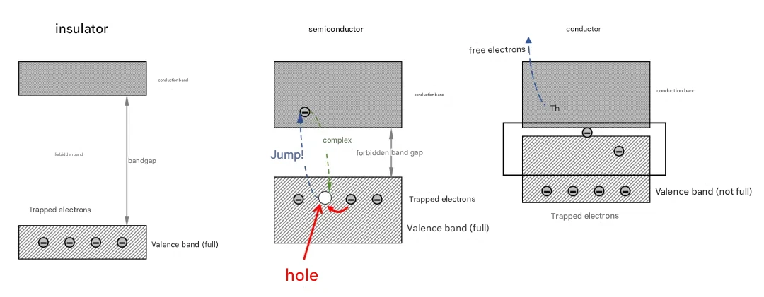
He believes that under the action of an external electric field, semiconductor conductivity is divided into conductivity with the participation of "holes" (i.e., P-type conduction) and conductivity with electron participation (i.e., N-type conduction). Many of the exotic properties of semiconductors are determined by both "holes" and electrons. Later, the band theory was further refined to systematically explain the essential differences between conductors, insulators, and semiconductors. Let's take a brief look at the band theory. As you have learned in middle school physics, objects are made up of molecules, atoms, and the outer shell of an atom is an electron. When the atoms of a solid object are close to each other, the electrons will be mixed together. Quantum mechanics believes that electrons can't stay in one orbit and "crashes". As a result, the orbit was split into several thin tracks. In quantum mechanics, this fine orbital is called an energy level. The wide orbit formed by multiple thin tracks squeezed together is called the energy band. Of the two bands, the lower one is the valence band, the upper one is the conduction band, and the middle one is the forbidden band. Between the valence band and the conduction band is a forbidden band. The distance of the forbidden band, which is the band gap (energy band gap).
Electrons move in a wide orbit and are macroscopically conductive. There are too many electrons, they are crowded, they can't move, and macroscopically they are not conductive. Some full orbits and empty orbits are very close together, and electrons can easily run from full orbits to empty orbits and move freely, which is called conductors. The two orbits are too far apart, the gap is too large, the electrons can't run through, and there is no way to conduct electricity. However, if you add an energy from the outside world, you can change this state.

If the band gap is within 5 electron volts (5 EV), an extra energy is added to the electron, and the electron can complete the leap and move freely, that is, conduction. This belongs to semiconductors. (The bandgap is about 1.12 eV for silicon and 0.67 eV for germanium.) If the band gap exceeds 5 electron volts (5EV), electrons cannot normally cross it, and it is an insulator. (If the outside world adds a lot of energy, it can also forcibly help it cross the past.) For example, air, air is an insulator, but high-voltage electricity can also break through air and form an electric current. It is worth mentioning that the "wide bandgap semiconductor" that we often hear about now is the third generation of semiconductor materials, including silicon carbide (SiC), gallium nitride (GaN), zinc oxide (ZnO), diamond, aluminum nitride (AlN), etc.
Their advantages are large bandgap width (>2.2EV), high breakdown electric field, high thermal conductivity, strong anti-radiation ability, high luminous efficiency, high frequency, can be used for high temperature, high frequency, radiation resistance and high-power devices, is the direction of the industry's current vigorous development. Earlier we mentioned electrons and holes. There are two types of carriers in semiconductors: free electrons and holes. Free electrons are familiar to everyone, what is a hole?
Holes are also known as electron holes. At room temperature, due to thermal motion, a small number of energetic electrons at the top of the valence band may cross the band and move up into the conduction band and become "free electrons". After the electrons run, a "hole" is left behind. The rest of the electrons that are not promoted can enter this "hole" and generate an electric current. It should be noted that the hole itself is immobile, but the process of "filling the hole" produces a positive electric flow effect, so it is also regarded as a carrier.
In 1931, Charles Thomson Wilson proposed a physical model of semiconductors based on band theory. In 1939, the Soviet physicist A.S. Davydov (A.S. Давыдов), the British physicist Nevill Francis Mott (Nevill Francis Mott), and the German physicist Walter Hermann Schottky (Walter Hermann Schottky) contributed to the basic theory of semiconductors. Davydov was the first to recognize the role of a few carriers in semiconductors, while Schottky and Mott developed the famous "diffusion theory". Based on the contributions of these bigwigs, the foundation of the basic theory of semiconductors has been gradually laid.
The birth of the transistor
After the birth of the ore geophone, scientists found that the performance of the geophone has a great relationship with the purity of the ore. The higher the purity of the ore, the better the geophone will perform. Therefore, many scientists have carried out purification research on ore materials (such as lead sulfide, copper sulfide, copper oxide, etc.), and the purification process has been continuously improved.
In the 30s of the 20th century, Russell Shoemaker Ohl, a scientist at Bell Labs, proposed that a geophone made of purified crystal materials would completely replace an electron diode. (You know, at that time, the tube was in an absolute market dominance.) )
罗素·奥尔,他还是现代太阳能电池之父
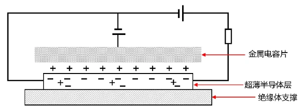
After testing more than 100 materials one by one, he decided that silicon crystals were the most ideal material for geophones. To test his conclusions, he refined a high-purity silicon crystal fusion with the help of his colleague Jack Scaff. Because Bell Labs didn't have the ability to cut silicon crystals, Orr sent the fusion to a jewelry store to cut it into crystal samples of different sizes. Unexpectedly, one of the samples, after illumination, behaved as a positive electrode at one end and a negative electrode at the other end, which Orr named as the P and N regions, respectively. In this way, Orr invented the world's first semiconductor PN junction (P–N junction). During World War II, Western Electric, a subsidiary of AT&T, manufactured a batch of silicon crystal diodes based on purified semiconductor crystals. The small size and low failure rate of these diodes greatly improved the performance and reliability of Allied radar systems. Orr's invention of the PN junction and the excellent performance of silicon crystal diodes strengthened Bell Labs' determination to develop transistor technology. In 1945, William Shockley of Bell Labs, after communicating with Russell Orr, drew the band diagram of P-type and N-type semiconductors based on band theory, and on this basis, proposed the "field effect hypothesis"
. 
肖克利的场效应设想
After testing more than 100 materials one by one, he decided that silicon crystals were the most ideal material for geophones. To test his conclusions, he refined a high-purity silicon crystal fusion with the help of his colleague Jack Scaff. Because Bell Labs didn't have the ability to cut silicon crystals, Orr sent the fusion to a jewelry store to cut it into crystal samples of different sizes. He hypothesized that the internal charge of the silicon wafer could move freely, and if the wafer was thin enough, under the influence of applied voltage, electrons or holes in the silicon wafer would emerge on the surface, greatly increasing the conductivity of the silicon wafer, thus achieving the effect of current amplification. Based on this vision, on December 23, 1947, John Bardeen and Walter Bratton of Bell Labs built the world's first semiconductor triode amplifier. That is, the following very strange and shabby-looking thing:
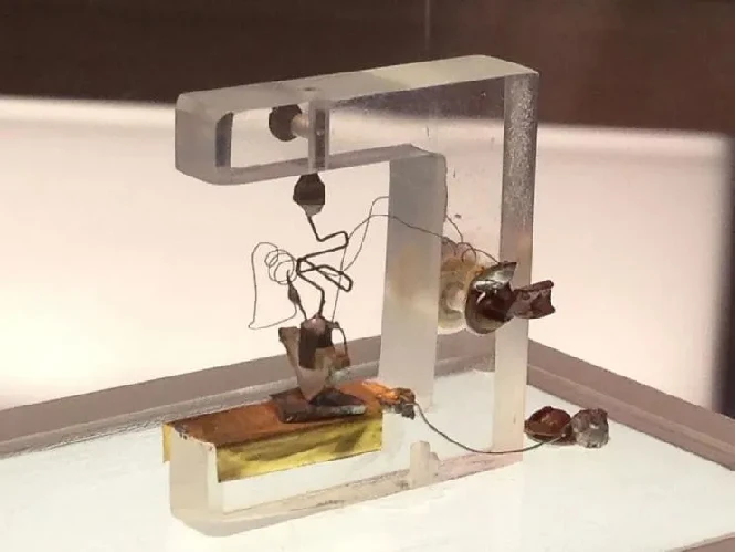
世界上第一个晶体管(基于锗半导体)
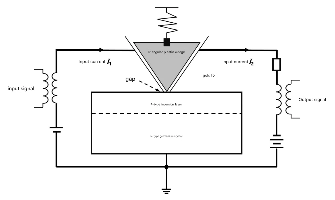
晶体管的电路模型
According to the experimental records, this transistor can achieve "voltage gain of 100, power gain of 40, and current loss of 1/2.5......", which is very good.
In naming it, Bardeen and Bratton argue that the device's ability to amplify signals is due to its resistance conversion characteristics, i.e., the signal goes from a "low-resistance input" to a "high-resistance output." So, they named it a trans-resistor. Later, it was abbreviated as transistor.
Many years later, Qian Xuesen, a famous scientist in China, set his Chinese translation name as: transistor.
I summarized that semiconductor properties are a special ability to conduct electricity (subject to external factors). Materials with semiconductor properties are called semiconductor materials. Silicon and germanium are typical semiconductor materials.
Microscopically, substances that are neatly arranged according to certain laws are called crystals. Silicon crystals have monocrystalline, polycrystalline, amorphous crystalline and other forms.
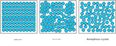
The crystal morphology determines the band structure, and the band structure determines the electrical properties. Therefore, silicon (germanium) crystals, as semiconductor materials, have such great application value. Diodes, triodes, and quadrudes are named from their functions. Electron tubes (vacuum tubes) and transistors (silicon transistors, germanium transistors) are named in principle. The transistor invented by Bardeen and Bratton should actually be called a point-contact transistor. As you can see from the image below, this design is too rudimentary. Although it achieves the amplification function, it is structurally fragile, sensitive to external vibrations, and not easy to manufacture, so it does not have the ability to be used commercially.
Shockley saw this flaw and began a retreat to study a new transistor design.
On January 23, 1948, after more than a month of hard work, Shockley proposed a new transistor model with a three-layer structure and named it the Junction Transistor.

肖克利的结式晶体管设计
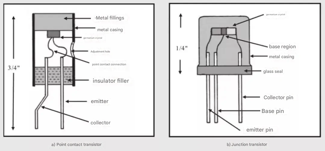
It was Morgan Sparks and Gordon Kidd Teal who helped Shockley make the final product. Special mention needs to be given to this Gordon Thiel. He found that replacing poly with monocrystalline semiconductors could lead to significant performance gains. Moreover, it was he who discovered that the Straight-pull method could be used to purify single metal crystals. This method has been used since then and is the most dominant single crystal fabrication method in the semiconductor industry. The birth of transistors is of great significance to the development of human science and technology. It has the ability of electron tubes, but overcomes all the shortcomings of large volume, high energy consumption, small magnification, short life and high cost of electron tubes. From the moment it was born, it was decided that it would achieve a complete replacement of the tube.
正在生产晶体管的工人
In the field of wireless communication, transistors, like electron tubes, can emit, detect, and amplify electromagnetic waves. In the field of digital circuits, transistors can also be more convenient to implement logic circuits. It has laid a solid foundation for the take-off of the electronics industry.
Later, the transistor family grew
█IC
The advent of transistors made it possible to miniaturize electrical circuits.
In 1952, Geoffrey Dummer, a well-known scientist at the Royal Radar Research Institute in the United Kingdom, noted at a conference:
"With the advent of transistors and the comprehensive study of semiconductors, it now seems conceivable that the electronic device of the future is a solid component with no connecting wires."
In August 1958, Kilby, a new employee at Texas Instruments, discovered that tiny circuits, made up of many devices, could be fabricated on a single wafer. In other words, different electronic devices (e.g. resistors, capacitors, diodes, and transistors) can be made on silicon wafers and connected with thin wires.
Soon after, on September 12, Kilby succeeded in manufacturing a germanium chip circuit 7/16 inch long and 1/16 inch wide based on his own ideas, which was also the world's first integrated circuit.
This circuit is a single transistor oscillator with RC feedback, and the whole thing is glued to the glass slide, which looks very rudimentary. The devices of the circuit are connected by scattered thin wires. At the same time that Kilby was inventing the integrated circuit, another person also made a breakthrough in this field. That person was Robert Norton Noyce of Fairchild Semiconductor (who later founded Intel). Fairchild is a company co-founded by Silicon Valley's "Eight Traitors" (see: The Legend of Fairchild), which has strong strength in semiconductor technology. Jean Hoerni, one of the "Eight Traitors", invented the very important Planner Process. In this process, a layer of silicon oxide is added to the silicon wafer as an insulating layer. Then, a hole is made in this layer of insulating silicon oxide, and the devices that have been made with silicon diffusion technology are connected with an aluminum film. The birth of the planar process enabled Fairchild to manufacture high-performance silicon crystal transistors with extremely small sizes, and also made it possible to connect devices in integrated circuits. On January 23, 1959, Noyce wrote in his work notes: "By fabricating various devices on the same silicon wafer and connecting them together using a planar process, it is possible to create multifunctional electronic circuits. This technology can reduce the size and weight of the circuit, and reduce the cost. "
诺伊斯
After learning that Kilby had filed a patent for an integrated circuit, Noyce was very remorseful, believing that he was one step too late. However, he soon discovered that Kilby's invention was flawed. Kilby's integrated circuits are connected by flying wires, which simply cannot be mass-produced and lack practical value. Neuss's vision was to make a negative plate of all the circuits and components of an electronic device and then engrave it on a silicon wafer. Once this silicon wafer is engraved, it is the entire circuit and can be used directly to assemble the product. In addition, the evaporative deposition of metal can replace the hot-welded wires and completely eliminate the flying wires.
Fairchild's silicon crystal integrated circuit
On July 30, 1959, Neuss applied for a patent based on his own ideas: "Semiconductor device - wire structure". Strictly speaking, Neuss's invention is closer to integrated circuits in the modern sense. Neuss' design is based on a silicon-based planar process, while Kilbi's design is based on a germanium-based diffusion process. Relying on the advantages of Fairchild's silicon process, Neuss has made circuits that are indeed more advanced than Kirby. In 1966, the tribunal finally granted Kilby the invention of the idea of an integrated circuit (a hybrid integrated circuit) and the invention of an integrated circuit packaged into a chip in use today (an integrated circuit in the true sense of the word), as well as the invention of the manufacturing process. Kilby is known as "the inventor of the first integrated circuit", while Noyce was the one who "came up with the theory of integrated circuits suitable for industrial production". In March 1960, Texas Instruments reported that Jack. Kilby's design officially launched the world's first commercialized integrated circuit product, the 502 silicon bistable multi-resonant binary flip-flop, which was sold for $450. The famous Apollo moon landing program purchased millions of integrated circuits, making Texas Instruments and Fairchild a lot of money. The success of the aviation market has led to the expansion of the civilian market. In 1964, Zenith used integrated circuits in hearing aids, which was the first landing of integrated circuits in the civilian field. Everyone should be familiar with the story after that. With the joint efforts of materials, processes and processes, the number of transistors in integrated circuits continues to increase, the performance continues to improve, and the cost gradually decreases, and we have entered the era of Moore's Law.

Moore's Law: The number of transistors that can fit on an integrated circuit doubles approximately every 18 months, and the performance doubles. The development of large-scale and ultra-large-scale integrated circuits based on integrated circuits has paved the way for the emergence of semiconductor storage and microprocessors. In 1970, Intel introduced the world's first DRAM (Dynamic Random Access Memory) integrated circuit, the 1103. The following year, they launched the Intel 4004, the world's first programmable chip that includes combinators and controllers. The golden age of IT technology has officially begun.
█ The evolution of transistors
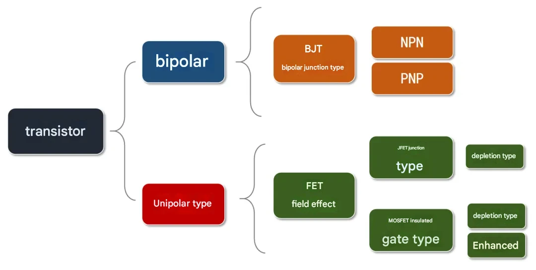
Let's go back and talk about transistors again. Since the advent of transistors, there have been many major changes in their form. In a nutshell, it is mainly from bipolar to unipolar. In the case of unipolar type, from FET to MOSFET. From a structural point of view, it is from PlanarFET to FinFET to GAAFET.
Bipolar, unipolar
The junction transistor invented by Shockley in 1948 is called a bipolar junction transistor (BJT) because it uses two carriers, holes and electrons, to participate in electrical conduction.
BJT transistors are available in two configurations: NPN and PNP:
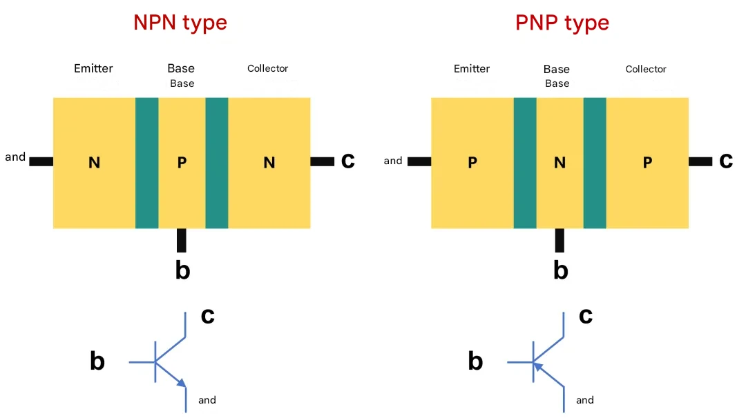
As we can see, a BJT transistor makes two PN junctions that are very close to each other on a semiconductor substrate. Two PN junctions divide the entire semiconductor into three parts, the middle part is the base, and the two sides are the emitter and collector. The working principle of BJT transistors is more complex, and it is rarely used nowadays, so I will not go into it for the sake of space. In essence, the main function of this transistor is to make the collector produce a large current change through a small current change in the base, which has an amplifying effect. The author mentioned logic circuits earlier. It is a combination of a diode and a BJT transistor, and is called a DTL (Diode-Transistor Logic) circuit. Later, TTL (Transistor-Transistor Logic) circuits were built entirely of transistors. The advantages of BJT transistors are their high operating frequency and strong driving capability. However, it also has drawbacks, such as high power consumption and low integration. Its manufacturing process is also more complex, and there are some drawbacks to the use of flat technology. As a result, over time, a new type of transistor began to emerge, known as the Field Effect Transistor (FET). In 1953, Ian Ross and George Dacey of Bell Labs collaborated to produce the world's first prototype of a junction field effect transistor (JFET).
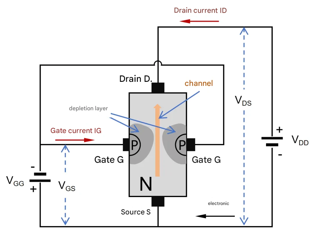
JFET(结型场效应晶体管),此为N沟道
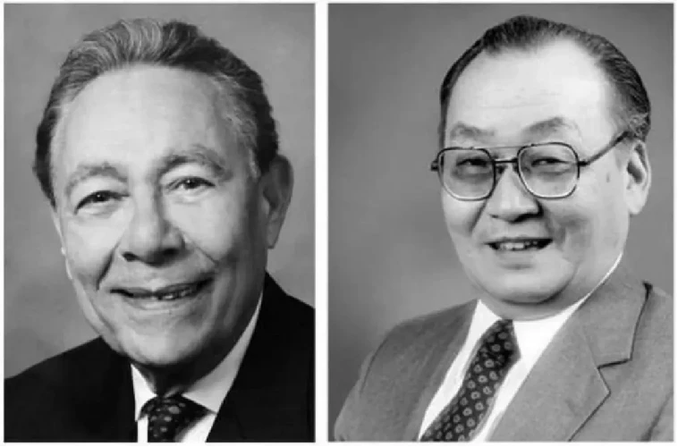
JFET is a semiconductor device with a three-pole (three-terminal) structure, including a source, drain, and gate. JFETs are divided into N-channel (N-channel) JFETs and P-channel (P-Channel) JFETs. The former is an N-shaped semiconductor with two P-type semiconductors on either side (as shown in the picture above). The latter is a P-shaped semiconductor with two N-type semiconductors on both sides. The working principle of JFET is simply to control the PN junction between the gate and the channel, and thus the depletion layer, by controlling the voltage between gate G and source S (VGS in the figure) and the voltage between drain D and source S (VDS in the figure). The wider the depletion layer, the narrower the channel, and the greater the channel resistance, the smaller the drain current (ID in the diagram) that can be passed. The state in which the channel is completely covered by the depletion layer is called the pinch state. When a JFET transistor works, it requires only one type of carrier, so it is called a unipolar transistor. In 1959, a new type of transistor was born, which was the famous MOSFET (Metal-Oxide-Semiconductor FET). It was invented by Mohamed Atala (renamed Martin Atala), a scientist of Egyptian origin, and Dawon Kahng, a scientist of Korean origin.
MOSFET is also composed of source, drain and gate. The "M" in "MOS" means that the gate was originally implemented using metal. "O" means that the gate and substrate are isolated using oxide. "S" means that the MOSFET is implemented as a whole by semiconductor.
MOSFET transistor, also known as IGFET (In-sulated Gate FET, insulated gate field effect transistor).
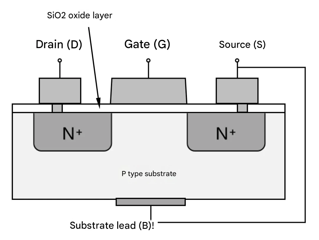
MOSFET(N型)
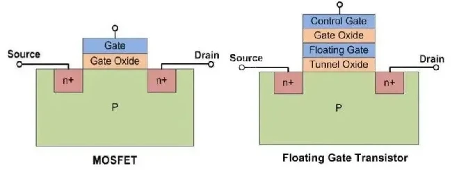
This MOSFET transistor is also divided into two types: "N-type" and "P-type", that is, NMOS and PMOS. According to the type of operation, it is also divided into enhanced and exhausted. Take the N-type MOS (more commonly used) in the figure above as an example. The P-type silicon semiconductor material was used as the substrate, and two N-type regions were diffused on the surface, and then a silicon dioxide (SiO2) insulation layer was covered on top of it. Finally, above the N zone, two holes were made by corrosion. Three electrodes are made on the insulating layer and in two holes by metallization: G (gate), S (source), and D (drain). The P-type silicon substrate has one terminal (B) that is connected to the source S by a lead. The working principle of a MOSFET is relatively simple: Normally, a neutral depletion region is formed between the N region and the substrate P due to the natural recombination of the carriers.
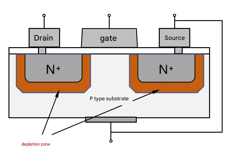
After a forward voltage is supplied to the gate, the electrons in the P region will accumulate under the action of the electric field under the silicon oxide of the gate, forming a region with electrons as many subons, that is, a channel.
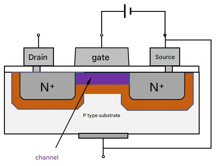
Now, if a voltage is applied between the drain and the source, the current will flow freely between the source and the drain, achieving a conduction state.

Gate G is like a gate that controls voltage, if a voltage is applied to gate G, the gate opens and current leads from source S to drain D. When the voltage on the gate is removed, the gate closes and the current cannot pass through.
In particular, it should be pointed out that in 1967, Jiang Dayuan cooperated with Chinese scientist Shi Min to jointly invent the "floating gate" FGMOS (Floating Gate MOSFET) structure, which laid the foundation of semiconductor storage technology. Later, all flash memory, FLASH, EEPROM, etc., were based on this technology.
BJT, JFET, MOSFET have just been introduced, I'll draw a diagram first, don't mess up your thinking:
In 1963, Fairchild Semiconductor's Frank Semiconductor. Frank Wanlass and Chih-Tang Sah (of Chinese descent) first proposed the CMOS transistor. They combine PMOS with NMOS transistors and connect them into complementary structures with almost no quiescent current. This is also the origin of the "C" (Complementary) of CMOS transistors.
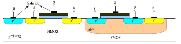
The biggest feature of CMOS is that the power consumption is much lower than that of other types of transistors. With the continuous development of Moore's Law, the number of transistors in integrated circuits is increasing, which makes the requirements for power consumption also increase. Based on the characteristics of low power consumption, CMOS has begun to become mainstream.
Today, more than 95% of integrated circuit chips are manufactured based on CMOS processes.
In other words, since the 1960s, the core architectural principles of transistors have been largely finalized. The integrated circuit ecology represented by CMOS, silicon (the natural stock of silicon far exceeds that of germanium, and its heat resistance is better than germanium, so it has become the mainstream), and planar technology has supported the rapid development of the entire industry for decades.
PlanarFET,FinFET,GAAFET
Although the core architecture principle has not changed, the form has changed.
Integrated circuits are constantly being upgraded, and processes and processes are constantly evolving. When the number of transistors reaches a certain scale, the process will force the transistors to "deform" to meet the needs of development. In the early days, transistors were mainly planar transistors (PlanarFETs). As the transistor becomes smaller, the length of the gate becomes shorter and shorter, and the distance between the source and drain gets closer together. When the process (that is, what we often call 7nm and 3nm, generally refers to the width of the gate) is less than 20nm, the trouble arises: the gate of the MOSFET is difficult to close the current channel, the restless electrons cannot be blocked, the leakage phenomenon occurs repeatedly, and the power consumption also increases.
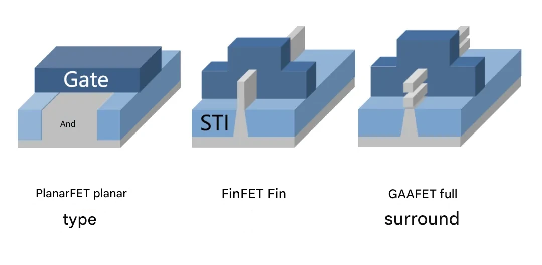
In order to solve this problem, in 1999, Professor Hu Zhengming, a Chinese-American scientist, officially invented the FinFET. Compared with the graphic design of PlanarFET, FinFET has directly become a 3D design and three-dimensional structure. Its current channel becomes a thin vertical slice like a fish's fin, clamped with a gate wrap on three sides. In this way, there is a relatively strong electric field, which improves the efficiency of the control channel and can better control whether electrons can pass through. Technology continues to evolve, and by the time it reaches 5nm, FinFETs will not work either. At this time, there was GAAFET (Wrap-Around Gate Technology Transistor). The full name of GAAFET in English is Gate-All-Around FET. Compared to FinFETs, GAAFET turns the gate and drain from fins into "small sticks" that pass vertically through the gate. In this way, from three to four contacts, and also split into several quadruple contacts, the gate control of the current is further improved. South Korea's Samsung has also designed another form of GAA, MBCFET (Multi-Bridge-Channel FET). MBCFET replaces nanowires in GAA with multilayer nanosheets, and the larger width of the sheet structure increases the contact surface, while retaining all the original advantages while minimizing complexity.
At present, the major chip companies in the industry are still in-depth research on the form upgrade of transistors, in order to find better innovations to support the development of chip technology in the future.
█ Epilogue
In general, whether it is an electron tube (vacuum tube) or a transistor, it is a small component that uses electricity to control electricity. Transistors are based on semiconductor materials, so they can be made small enough. This is the reason why chips (integrated circuits) can achieve "extremely small size, great ability". The properties of semiconductor materials, as well as the role of transistors, seem very simple. It is hundreds of millions of such simple "gadgets" that support the development of human digital technology and push us towards the era of digital intelligence.
Send Inquiry