


Integrated Processes in Chip Manufacturing
Oct 29, 2024
Leave a message
0040-02544 Upper Body, Dps Metal
0020-33806 Upper Chamber Dps + Poly
Integrated process modules
Process requirements for integrated circuits
Full reliability:Integrated circuits need to operate stably in a variety of environments and conditions, including extreme conditions such as high temperatures, low temperatures, and high humidity.
Reliability also involves the longevity of a circuit, which is the ability of a circuit to maintain good performance over a long period of time.
Stable high performance:High performance means that the circuit has fast processing speed, low power consumption, and high integration. As technology continues to advance, so does the demand for high performance.
Low-cost price: The production cost of integrated circuits needs to be controlled within a reasonable range to meet market demand. Ways to reduce costs include improving production efficiency, optimizing processes, and more.
The challenges of miniaturization
Increase current density and electric field strength: As the transistor size decreases, the current density and electric field strength increase accordingly, which can lead to reduced circuit reliability. The increase in leakage current is also a problem that needs to be addressed.
Increased complexity: More complex structures are required to address the problems posed by miniaturization, which increases the complexity and cost of the process. More processes and longer manufacturing cycles also increase the uncertainty of production.
Structural modules of LSI
Process integration: Process integration is the combination of various basic processes to manufacture the required integrated circuits. Different manufacturers may have different names, but they are essentially integrating multiple process steps together.
Basic processes and modules: The manufacturing of integrated circuits involves several basic processes, such as lithography, etching, ion implantation, etc., etc. These basic processes can be further divided into different modules, such as transistor fabrication modules, cabling modules, etc.
Interaction between modules: There is a mutual influence between the processes of each module, especially the processing conditions and atmosphere of the pre- and post-processes. Therefore, these interrelationships need to be considered in the process design to ensure the quality and performance of the final product.
The following diagram shows the important problems faced by the basic process in each module process:
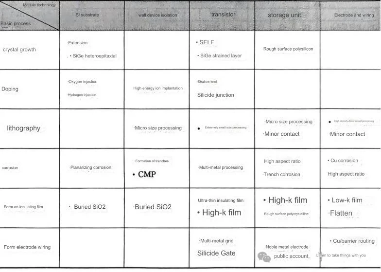
Basic integrated process
The fabrication of integrated circuits is a highly delicate and complex process that relies on a series of precisely controlled process steps, which are often organized into different modules.
The following is a detailed explanation of the basic processes for n-groove MOS transistor fabrication, which together form the manufacturing process at the 3 micron technology node.
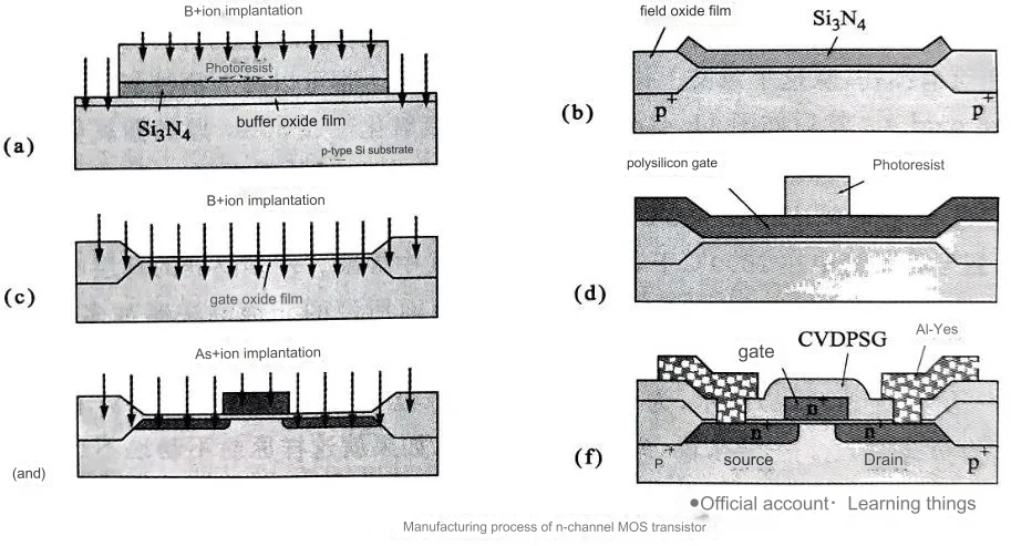
1. Buffer the formation of oxide films
Step description: A p-type (100) crystal orientation with a resistivity of 10Ω·cm Si substrate wafer is placed in a quartz tube and oxidized in oxygen heated to 1000 °C for 60 minutes to form a 50 nm thick SiO2 layer, which is called dry oxygen oxidation. This layer of SiO2 film is called a buffer oxide film.
Purpose: To provide a flat and stable substrate for subsequent processes while protecting the Si substrate from damage during subsequent processing.
2. Formation of silicon nitride layers
Step description: Ammonia (NH3) is reacted with dichlorosilane (SiH2Cl2) gas in a quartz tube heated to 800°C, and the entire surface of the Si substrate is covered with a 120nm thick layer of silicon nitride (Si3N4), which is called CVD method (chemical vapor deposition).
Purpose: To act as a masking layer for subsequent processes to protect part of the Si substrate from oxidation and other treatments.
3. Ion implantation and lithography
Step description: First, the photoresist resin is selectively retained by photoetching, and then placed in a fluorine-containing plasma to remove the Si3N4 film that is not covered by the photoresist. Next, the boron ion B+ is accelerated by 75keV to collide with the wafer and cause it to invade the silicon wafer.
Purpose: To form a channel blocking layer by ion implantation to prevent leakage current between adjacent devices.
4. Formation of field oxide films
Step description: After removing the remaining photoresist, the surface is washed with aqua regia and dilute hydrofluoric acid, and then oxidized in water vapor at 1000 °C for 6 hours to form a 1 μm thick SiO2 film (called field oxide film), which is called wet oxygen oxidation method.
Purpose: To form an insulating layer on a Si substrate to isolate different circuit components.
5. Gate oxide film formation and sacrificial oxidation
Step description: After removing the Si3N4 layer and part of the SiO2 layer below, dry oxygen oxidation at 50nm is carried out, and then this layer of SiO2 (called sacrificial oxide film) is removed again, and finally a gate oxide film with a thickness of 50nm is formed.
Objective: To provide a high-quality insulation layer for the gates of MOS transistors. The sacrificial oxidation step is used to remove the SiO2 layer that has been damaged by the pretreatment.
6. Formation of gate electrodes
Step description: A 400nm thick polycrystalline silicon film is deposited on a Si substrate, and then phosphorus is doped to reduce the resistivity. Next, the polycrystalline silicon film is etched by photoetching to form a gate electrode.
Purpose: To act as the gate of a MOS transistor to control the current breaking between the source and drain.
7. Source and drain formation
Step description: As+ is injected into the Si substrate by ion implantation to form n-type source and drain. An activation heat treatment (annealing) is then undertaken, which makes the injected ions electrically active.
Purpose: To provide current input and output terminals for MOS transistors.
8. CVD-PSG Deposition and annealing of membranes
Step description: Deposition a 600 nm thick CVD-SiO2 film (called CVD-PSG film) containing a few percent phosphorus. The surface is then vitrified by annealing in a furnace with POCl3.
Objective: To provide a flat and stable substrate for the subsequent aluminum electrode, and at the same time reduce the softening temperature of SiO2 for subsequent processing.
9. The formation of contact holes and the deposition of aluminum electrodes
Step description: The contact hole is opened on the CVD-PSG film by photoetching, and then a layer of aluminum electrode film containing 1%~2% Si with a thickness of 800nm is deposited. Purpose: To connect the aluminum electrode with the source, drain and gate electrode through contact holes to form a complete circuit connection.
Together, these steps form the basic manufacturing process for n-channel MOS transistors. In actual production, multiple cleaning, inspection and testing steps are required to ensure the quality and performance of the final product. As technology continues to advance, these process steps are constantly being optimized and improved to accommodate higher levels of integration and more stringent performance requirements.
Substrate structure
Wafer structure
In the development of integrated circuits, the quality of Si substrate, as the core material, has a crucial impact on the performance of the device. In the early days, integrated circuits mainly used monocrystalline silicon prepared by the Cheklauski (CZ) method or the suspension melting (FZ) method. Most of these monocrystalline silicons are in the (100) direction because this direction has the best MOS transistor performance.
In the manufacture of CMOS devices, a well-well structure is required in order to form both n-groove and p-groove transistors on the same substrate. The well structure enables the coexistence of N-groove and P-groove transistors by forming p-type and n-type substrates under the transistor, respectively.
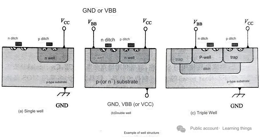
With the development of technology, the well structure has also undergone an evolution from a single well to a double well to a triple well, increasing the degree of design freedom, enhancing the ability to resist external noise, and improving the ability to suppress latch-up (short circuits caused by a source-drain and a thyristor structure consisting of a trap and substrate).
SOI substrates
SOI (Insulating Film Silicon Laminate) substrates are a competitive technology, and although there are not many devices currently using SOI substrates, their potential is huge. The development of SOI substrates began in the 60s of the 20th century with the aim of improving radiation resistance and enabling high-speed operation. Among them, the silicon-sapphire (SOS) structure has been partially put into practical use, but it has not yet become mainstream due to problems such as crystallinity, price and process compatibility. 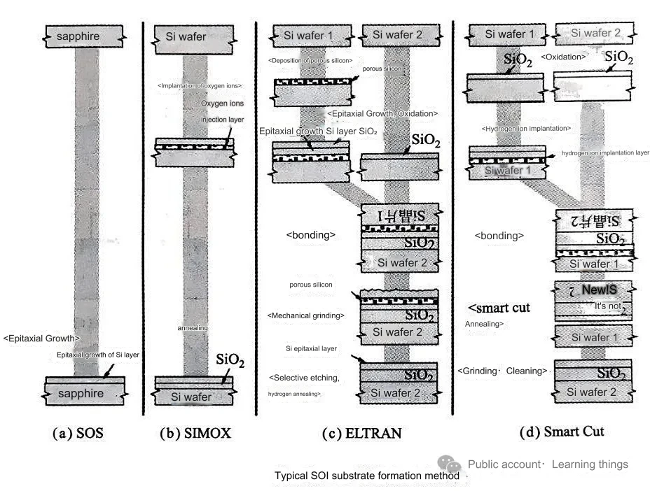
Later, the Oxygen Injection Isolation (SIMOX) technique was developed to achieve the SOI structure by forming a SiO2 buried layer under the surface of the Si substrate. However, SIMOX technology has not yet become mainstream due to the reduction of throughput due to the large amount of oxygen injection, as well as problems such as SiO2 thickness limits and crystallization defects.
In recent years, wafer bonding technology has been developed as an alternative to SOS and SIMOX. Wafer bonding technologies, including the ELTRAN and Smart Cut methods, have achieved high-quality SOI substrate preparation by forming porous silicon, depositing epitaxial layers, or using hydrogen ion implantation layers for mechanical separation. These SOI substrates have already begun to be used in high value-added products such as ultra-high-speed processors, where they can effectively reduce the parasitic capacitance of the substrate, thus contributing to high speed and low power consumption.
END
Send Inquiry