


Wet etching, dry etching, and ALE : The technological logic of three generations of etching processes
Jun 05, 2026
Leave a message
Etching is one of the core micro- and nano-fabrication technologies in modern semiconductor manufacturing. Its essence is the controlled and selective removal of material from the surface to construct the microstructures and functional patterns required for devices. As the feature size of integrated circuits continues to advance towards the nanoscale, etching is no longer a simple material removal process but has gradually evolved into a critical step determining device dimensional accuracy, interface quality, and the integrity of the three-dimensional structure. In advanced logic devices, memory chips, MEMS, and power semiconductors, etching processes directly affect trench morphology, gate structure, contact hole size, and the reliability of subsequent thin-film deposition and interconnection processes. Therefore, its process control capability has become one of the important indicators for measuring the level of chip manufacturing.
wet etching and dry
etching. Wet etching mainly relies on the chemical reaction between a liquid chemical solution and the material surface to dissolve the material. The reaction products then diffuse into the solution system and are carried away. This method is simple in equipment, low in cost, and has a high etching rate and excellent selectivity in some material systems, so it was widely used in early integrated circuit manufacturing. However, because etching particles have the characteristic of uniform diffusion in liquids, the material is often etched simultaneously in both the vertical and lateral directions, easily producing obvious lateral etching phenomena, which is difficult to meet the high-precision pattern transfer requirements of deep submicron devices.
In contrast, dry etching utilizes active particles, free radicals, and high-energy ions in a plasma environment to remove materials, and is currently the mainstream technology in advanced semiconductor manufacturing. Plasma is essentially a partially ionized gas system containing various active components such as electrons, ions, neutral free radicals, and excited-state particles. Under the influence of a radio frequency electric field, the etching gas is excited to form a highly reactive plasma environment. Different particles etch materials through chemical reactions, ion bombardment, or synergistic effects. Compared with traditional wet etching, the biggest advantage of dry etching is that it can significantly enhance the etching directionality through directional ion bombardment, thereby forming steeper sidewall structures. This is particularly crucial for high aspect ratio devices such as FinFET, 3D NAND, and TSV.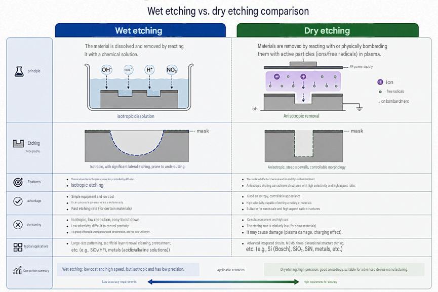
Depending on the process environment, etching can generally be divided into two major systems: wet etching and dry etching. Wet etching mainly relies on the chemical reaction between a liquid chemical solution and the material surface to dissolve the material. The reaction products then diffuse into the solution system and are carried away. This method is simple in equipment, low in cost, and has a high etching rate and excellent selectivity in some material systems, thus it was widely used in early integrated circuit manufacturing. However, because etching particles have an isotropic and uniform diffusion characteristic in liquids, the material is often etched simultaneously in both the vertical and lateral directions, easily resulting in significant lateral etching, which is difficult to meet the high-precision pattern transfer requirements of deep submicron devices.
In contrast, dry etching utilizes active particles, free radicals, and high-energy ions in a plasma environment to remove materials, and is currently the mainstream technology in advanced semiconductor manufacturing. Plasma is essentially a partially ionized gas system containing various active components such as electrons, ions, neutral free radicals, and excited-state particles. Under the influence of a radio frequency electric field, the etching gas is excited to form a highly reactive plasma environment, where different particles achieve material etching through chemical reactions, ion bombardment, or synergistic effects. Compared to traditional wet etching, the biggest advantage of dry etching is its ability to significantly enhance etching directionality through directional ion bombardment, thereby forming steeper sidewall structures. This is particularly crucial for high aspect ratio devices such as FinFETs, 3D NAND, and TSVs.
Etching morphology is typically
evaluated using the degree of anisotropy as a core indicator. Ideally, material is removed only along the vertical direction, with sidewalls remaining nearly vertical, achieving high-fidelity pattern transfer. However, in actual processes, lateral etching is often unavoidable due to factors such as active particle diffusion, sidewall reactions, and ion scattering. The difference between the longitudinal and lateral etching rates is usually used to measure process directionality: when lateral etching is minimal and etching primarily occurs along the vertical direction, the process exhibits high anisotropy; while when the lateral and longitudinal etching rates are similar, it exhibits typical isotropic characteristics. As device dimensions continue to shrink, high anisotropy has become an important development direction for advanced etching processes. However, excessively steep sidewalls can also lead to difficulties in subsequent thin film coverage, metal filling defects, and interface stress concentration. Therefore, modern processes emphasize precise control of sidewall angles and contour morphology, rather than simply pursuing an absolutely vertical structure.
Besides directionality, selectivity is also an important parameter for evaluating etching performance. Selectivity reflects the difference in etching rates between the target material and the mask material, essentially demonstrating the process's ability to distinguish between different materials. In actual manufacturing, the mask layer needs to remain sufficiently intact before pattern transfer; therefore, a higher selectivity effectively reduces mask loss, improves dimensional control accuracy, and minimizes process window fluctuations. Generally, etching mechanisms dominated by pure chemical reactions typically have higher selectivity because the etchant reacts only with specific materials. While physical etching, primarily based on ion bombardment, offers excellent directionality, the lack of chemical selectivity in material removal means that the mask and substrate are often bombarded simultaneously, leading to a decrease in selectivity. Therefore, in practical process development, a balance needs to be struck between anisotropy and selectivity.
Most modern advanced etching technologies employ a synergistic coupling of physical bombardment and chemical reactions to balance directionality and selectivity. For example, reactive ion etching (RIE), inductively coupled plasma etching (ICP), and deep reactive ion etching (DRIE) all achieve synergistic control of ion energy and chemical activity by adjusting RF power, bias voltage, plasma density, and reactive gas composition. Bosch's deep silicon etching process, through alternating etching and sidewall passivation, can achieve structures with extremely high aspect ratios and is widely used in MEMS and advanced packaging. In recent years, with the increasing demand for atomic-level manufacturing, atomic layer etching (ALE) has gradually become a research hotspot. Through a cyclic mechanism of "surface adsorption-self-limiting reaction-quantitative removal," it achieves material removal with near-single-atom-layer precision, providing crucial technical support for future advanced process nodes of 2 nm and below.
Overall, the development of etching technology has gradually moved from traditional large-scale material processing to a stage of precise atomic-scale control. In the future, with the development of 3D integration, heterogeneous packaging, and new semiconductor materials, higher demands will be placed on etching processes in terms of high aspect ratio structure control, low-damage processing, ultra-high selectivity, and atomic-level precision. The collaborative development of plasma physics, surface and interface chemistry, and intelligent process control will continue to drive the evolution of advanced etching technology towards higher precision and reliability.
Send Inquiry