


How bonding technology allows semiconductors to be stacked higher and higher
May 28, 2026
Leave a message
In the semiconductor industry's pursuit of higher performance and lower power consumption, simply shrinking transistor size has become increasingly difficult. So, engineers have adopted a different approach: since horizontal shrinking is not feasible, they've opted for vertical stacking-building different chips layer by layer, like constructing a skyscraper. The core technology that allows chips to "grow taller" is bonding technology.
What is bonding? In the world of chips,
bonding, often referred to as "super glue," simply means permanently bonding two or more wafers (or chips) together, simultaneously achieving electrical interconnection between them. This is something ordinary glue cannot accomplish. Bonding requires a tight bond between the surfaces of two materials at the atomic scale, ensuring both mechanical strength and unimpeded electrical signal transmission.
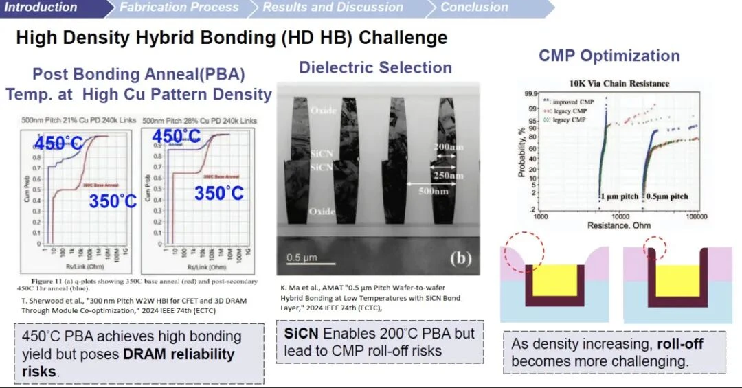
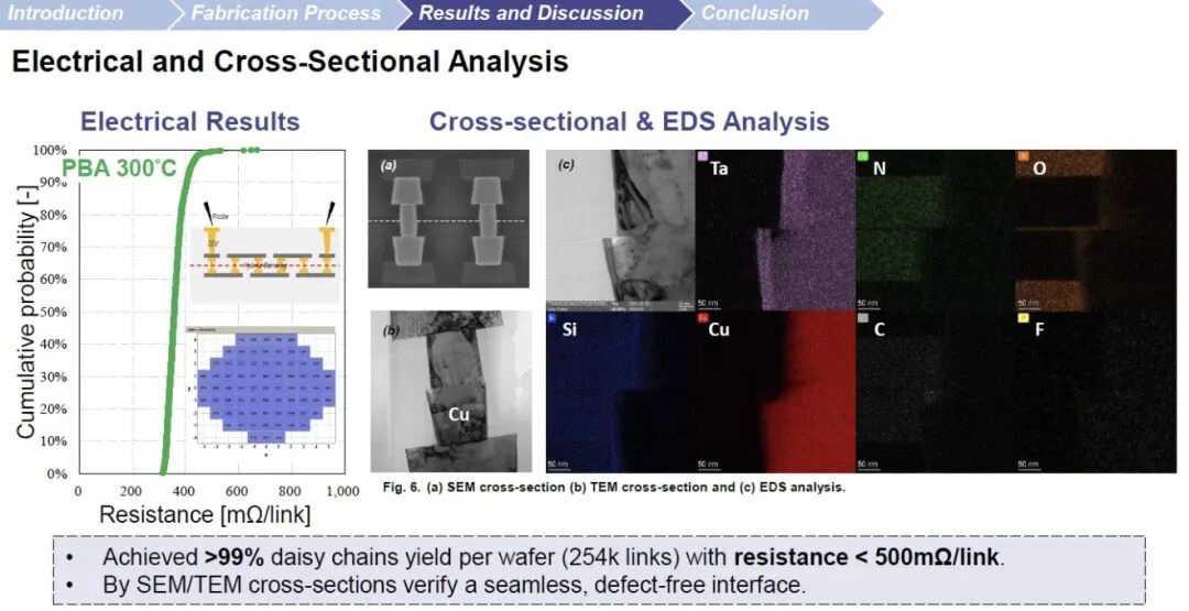
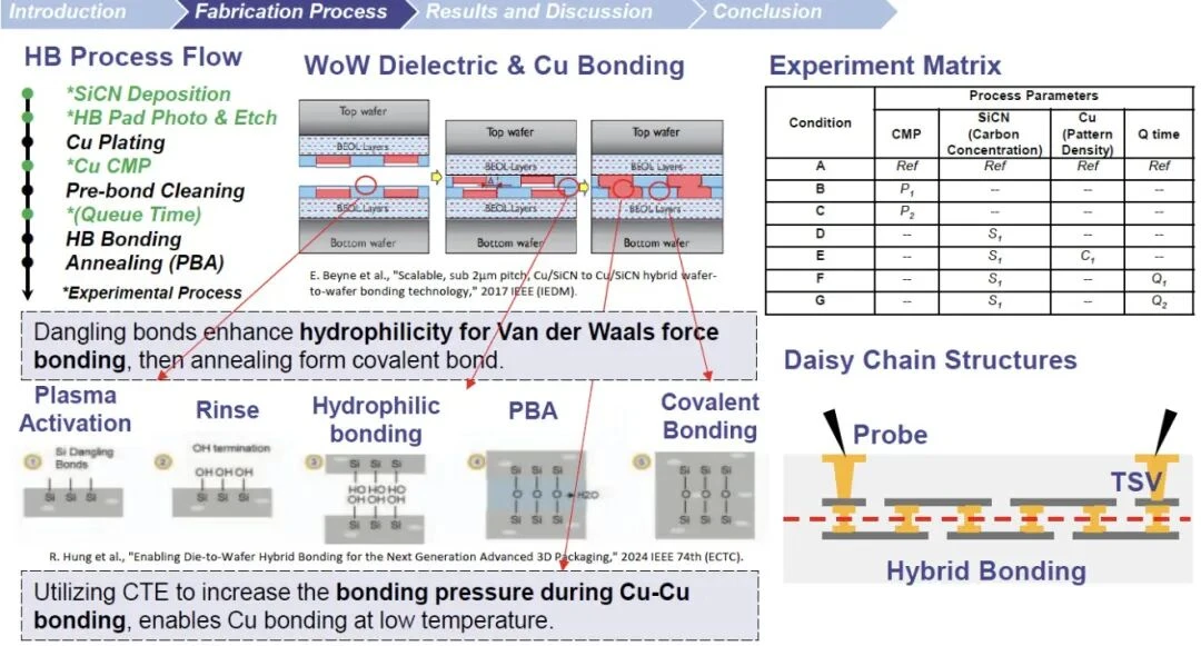
Depending on the application, bonding technologies are mainly divided into two categories: direct bonding (also called fusion bonding) and hybrid bonding. Direct bonding involves bonding two clean wafers through surface molecular forces, followed by high-temperature annealing to enhance the bond strength. It is often used in applications where precise electrical alignment is not required. Hybrid bonding goes a step further, embedding both metal (usually copper) and an insulating medium at the bonding interface. This allows the two wafers to be physically bonded while the metal pads also directly conduct electricity. This technology enables extremely high interconnect density and is the core of advanced packaging.
Four Major Applications: From Cameras to Processors
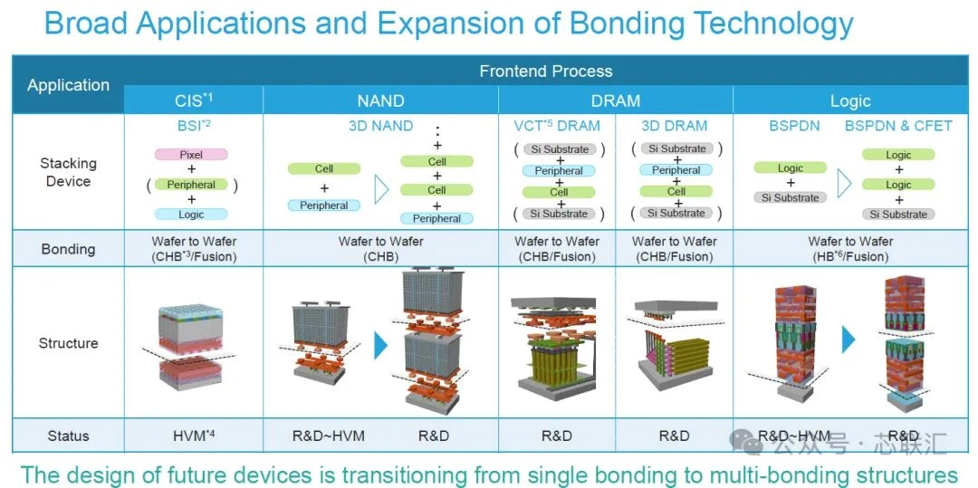
As seen in the images, bonding technology has permeated the manufacturing of many mainstream chips.
CIS (CMOS Image Sensor): This is one of the earliest applications of bonding technology in mass production. Traditional CIS fabricates the pixel array and processing circuitry on the same wafer. Back-illuminated (BSI) CIS, however, fabricates the pixel layer and logic circuitry layer separately on two wafers, then bonds them face-to-face. The advantage of this is that each pixel can occupy its own photosensitive area, unaffected by circuitry, significantly improving image quality. The image shows CIS using wafer-to-wafer hybrid bonding (CHB/Fusion), which has entered mass production (HVM).
NAND Flash Memory: 3D NAND itself stacks memory cells vertically. However, its peripheral circuitry (driver, decoder, control logic) still occupies a considerable chip area. To achieve higher storage density, manufacturers began fabricating the peripheral circuitry on a separate wafer, then bonding it to the memory cell wafer. This allows the memory cells to be stacked higher, without the peripheral circuitry taking up space. The image shows that NAND bonding is in the R&D to HVM stage.
DRAM memory: Traditional DRAM places the memory cells and peripheral circuitry on the same plane; as capacity increases, the chip area also expands. VCT (Vertical Channel Transistor) DRAM is exploring stacking memory cells on top of peripheral circuitry to achieve true 3D DRAM. This also relies on wafer-to-wafer bonding technology and is currently in the R&D stage.
Logic chips: This is the most cutting-edge application of bonding technology-Back-side Power Distribution Network (BSPDN). Traditional chips have their power supply network and signal lines crammed onto the front of the chip, resulting in not only congested wiring but also voltage drops. Back-side power distribution technology moves the entire power supply network to the back of the chip, bonding the wafer carrying the power supply network to the wafer carrying the transistors. This design can significantly improve logic density and performance and is currently in the critical R&D phase.
from single-bonding to multi-bonding,
states: "Future device design is moving from single-bonding to multi-bonding structures." This means that future chips may not just have two layers, but three, four, or even more-for example, logic layers, memory layers, power supply layers, and heat dissipation layers stacked together. Each bond requires extremely high alignment precision (nanometer-level), perfect interface quality, and reliable interconnect resistance control. This presents unprecedented challenges to bonding equipment, process cleanliness, and thermal budget management.
In conclusion,
bonding technology is no longer a fancy laboratory process; it is reshaping the entire semiconductor industry, from image sensors to processors, from memory to flash memory. As Moore's Law falters in the planar direction, bonding technology has allowed chips to find new growth space in the vertical direction. In the future, the chips in your mobile phone, the AI accelerators in data centers, and the computing platforms for autonomous driving may all be layers of intricate "chip crepes." And the knife that cuts through these layers is that thin yet unbreakable bonding interface.
Send Inquiry