


Chip Manufacturing: Thin Film Deposition
Jul 22, 2025
Leave a message
In the microscopic world of chips, transistors need to be insulated and metal wires need to be connected by conductive layers - these nanometer thickness (1 nanometer = billionth of a meter) thick film is like a brush that "draws circuits" for chips. The three core thin film deposition technologies in semiconductor manufacturing: ALD, CVD, PVD, each play an irreplaceable role.
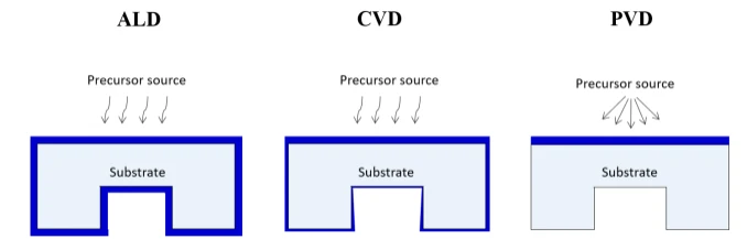
Comparison of the three major technologies
|
Characteristic |
Atomic layer deposition (ALD) |
Chemical vapor deposition(CVD) |
Physical vapor deposition (PVD) |
|
Deposition rate |
Extremely Slow (1-10 nm/minutes) |
Medium (10-100 nm/minutes) |
Extremely Fast (100 nm-1 μm/minutes) |
|
Coverage capabilities |
Perfect conformal (100% coverage of deep trenches) |
Medium conformal (gas transmission-dependent) |
Straight Line Coverage (Surface Coat |
|
Applicable materials: |
Oxides/nitrides/metal oxides/metals |
Oxide/nitride/metal compounds |
Metal/alloy partial oxides |
|
Process temperature |
Wide temperature (50-400°C) |
High temperature (300-1000°C) |
Low temperature (room temperature -500°C) |
|
Deposition principle |
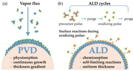
Self-limiting atomic layer growth (stacked layer by layer like a wall) |
Deposition of gas-phase chemical reactions (e.g., gas "snow") |
Physical sputtering/evaporation (like painting) |
|
Directionality |
Isotropy (uniform coverage in all directions) |
Isotropic (gas can penetrate into crevices) |
Straight direction (spray only to the direct view area) |
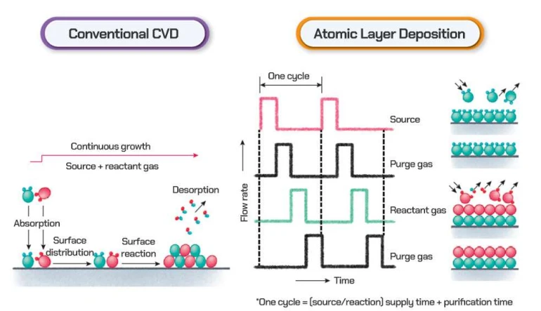
ALD: Precision devices
Advantage: Atomic-scale uniform coating on the surface of 3D structures (e.g. FinFET fins).
Typical applications: high-k gate dielectric layer for chips below 7nm, capacitive insulation layer for memory chips. Cost: Slow speed and high cost.
2. CVD:Large-scale films
Advantages: Efficient deposition of complex compounds (e.g. silica insulation, silicon nitride passivation layer).
Innovation direction: Plasma-enhanced CVD (PECVD) reduces temperature and reduces damage to the bottom layer.
PVD: Metal Interconnection
Advantages: Rapid deposition of copper/aluminum wires, titanium/tantalum barriers.
Fatal flaw: Cannot cover deep via sidewalls → Requires use with ALD/CVD.
0021-02395 REV.B INSERT RING,ALUMINUM DxZ SACVD
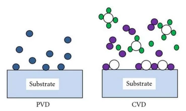
Engineering challenge: When the chip structure has a depth-to-width ratio of 40:1 (equivalent to a wellhead diameter of 1 meter and a well depth of 40 meters), only ALD can completely cover the wellbore wall!
0010-37264 Cooldown Chamber Multi Slot Ass'y
Why do you need three technologies?
Accuracy requirements: The thickness of the transistor gate dielectric layer ≈ 12 atoms, which is not controllable without ALD.
Efficiency balance: The metal conductor layer is completed in 10 minutes with PVD, and ALD takes 10 hours.
Structural adaptability: planar structure → CVD/PVD ; 3D nanoholes → must be ALD.
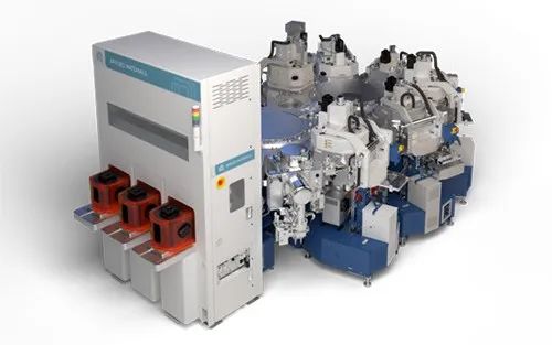
Consequences of film failure Uneven thickness:
the gate dielectric layer difference is 1 atom → transistor leakage increases by a hundredfold.
Covering defect: The deep hole sidewall is not covered → metal conductor short circuit.

Send Inquiry