


Chip Manufacturing: DPN Plasma Nitriding
Jun 12, 2025
Leave a message
In the sub-5nm chip manufacturing process, the thickness of the transistor gate dielectric layer has shrunk to less than 1 nanometer (about 5 atomic layers). At this time, conventional silica (SiO₂) acts like a thin veil of water leakage, and the leakage power consumption caused by electronic tunneling can account for up to 40% of the total power consumption.
The decoupled plasma nitriding (DPN) technology builds a "nano anti-theft net" by precisely injecting nitrogen atoms into the oxide layer, which not only blocks the channel of electronic leakage, but also opens up a new path for chip performance.
I,What's DPN?
DPN (Decoupled Plasma Nitridation) is a low-temperature plasma surface treatment technology, the core principle of which is to inject nitrogen atoms into the gate oxide layer in a controlled manner to form a nitrogen-rich interface. Unlike traditional thermal nitriding, the "decoupling" characteristics of DPN are reflected in:
Energy decoupling: The plasma energy is controlled independently (usually 100-500W) to prevent high-energy particles from damaging the silicon substrate.
Spatial decoupling: The plasma is confined by a magnetic field, so that the nitrogen atoms are mainly enriched on the upper surface of the oxide layer rather than the silicon/oxide interface, and the carrier mobility is protected.
Key technical indicators:
Nitrogen concentration: precise control of 5-10 atomic percentage (more than 15% will cause interface defects).
Thickness limit: Ultra-thin film processing of ≤10 angstroms (1 nm) can be realized, which is a necessary process for sub-5nm nodes.
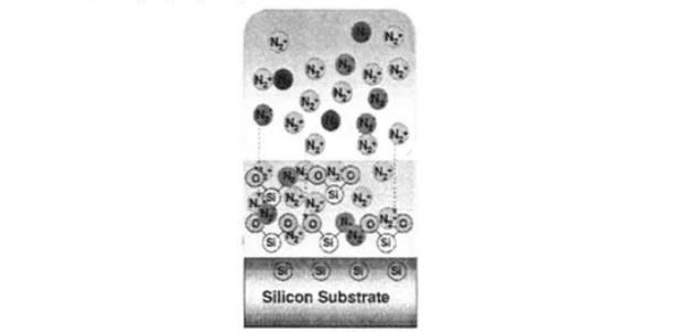
II. DPN Process
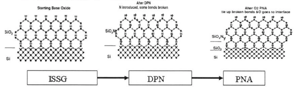
Taking the 28nm HKMG (High K Metal Gate) process as an example, the key steps of DPN are as follows: Oxide layer grows on a silicon substrate ISSG grows a thin layer of silicon dioxide as a nitriding substrate.
Plasma nitriding
Gas atmosphere: N₂/HN3 (main gas), Ar (dilute gas) are introduced, and the pressure is 35-70 mTorr. Plasma activation: RF power supply (200-600W) ionizes gas to generate highly reactive nitrogen ions (N⁺). Nitrogen permeation: Nitrogen ions penetrate the surface layer of SiO₂ and form a nitrogen-rich zone within 0.5 nm of the upper surface.
PNA
Rapid annealing (600-800°C) in the same vacuum chamber drives uniform diffusion of nitrogen atoms, repairs lattice damage, and reduces the density of the interfacial state.
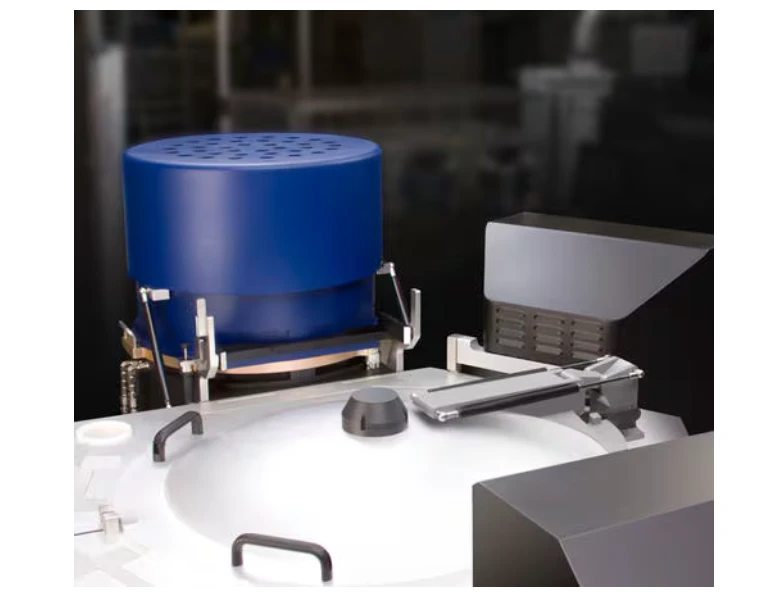
0040-09094 CHAMBER 200mm
III. There are four major roles of DPN in gate nitriding
1. Increasing the dielectric constant (k-value): When the nitrogen atom replaces the oxygen atom in SiO₂, it forms a Si-N bond (which is more polar than the Si-O bond), increasing the k-value from 3.9 to 4.5-7.0. Under the same capacitance, the physical thickness can be increased by 20%, which directly suppresses the quantum tunneling effect.
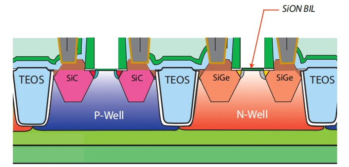
Gate leakage current suppression: In the 1 nm oxide layer, DPN nitrogen doping reduces the leakage current from 1000 A/cm² to 10 A/cm² (a 99% reduction). The principle is that the nitrogen atom raises the conduction band energy barrier of SiO₂, and the electrons need higher energy to tunnel.
3. Blocking dopant diffusion: The boron atoms of the PMOS gate easily penetrate the SiO₂, resulting in threshold voltage drift. The nitride layer acts as an "atomic filter", reducing the boron diffusion coefficient by 10³ times and ensuring the long-term stability of the device.
4. Optimize the interfacial state: By controlling the peak position of nitrogen (0.3 nm from the interface> to avoid nitrogen atoms from destroying the silicon suspension bond, the electron mobility is kept large.
Send Inquiry