


Why Use High-k Materials as Gate Dielectric Layer Materials?
Aug 15, 2024
Leave a message
0010-36522 EDGE RING
0040-02544 Upper Body, Dps Meta
Why Use High-k Materials as Gate Dielectric Layer Materials?
How did the gate dielectric layer develop? Why does the advanced process use high-k materials as the gate dielectric layer?
What is used for the gate dielectric layer of advanced nodes?
|
Technology Node |
Structural Features |
High-k Medium |
|
|
nMOS |
pMOS |
||
|
45 nm |
Planar |
HfO₂/ZrO |
HfO₂/ZrO |
|
32 nm |
Planar |
HfO₂ |
HfO₂ |
|
22 nm |
FinFET/Tri-gate |
HfO₂ |
HfO₂ |
|
14 nm |
FinFET/Tri-gate |
HfO₂ |
HfO₂ |
As shown in the table above, at the 45nm node and below, the HKMG (High-k Metal Gate) process is used, and the high-k material is used as the gate dielectric layer; Nodes above 45nm mainly use silicon oxide as the gate dielectric layer.
What is a gate dielectric layer?
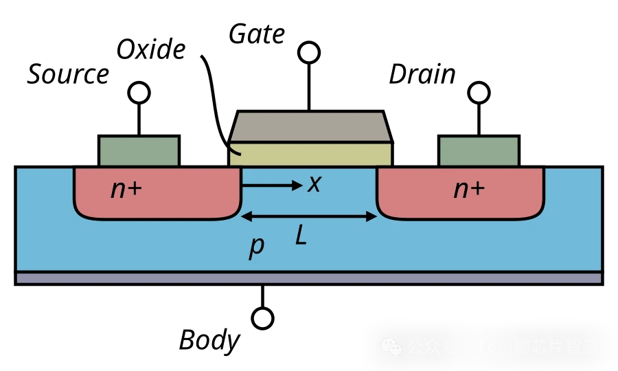
As shown in the figure above, the gray area at the top of the diagram represents the gate, and a voltage is applied to the gate to control the formation of a current channel between the source and drain. The light yellow layer below the gate represents the gate dielectric layer, isolating the gate and the single crystal substrate from direct current conduction.
What is Gate Leakage Current?
As the process node shrinks, the chip size decreases, and the gate oxide layer continues to thin, and when the gate dielectric layer is very thin (less than 2nm) or at high voltages, electrons pass through the dielectric layer through the tunneling effect, resulting in a leakage current between the gate and the substrate.
Problems caused by leakage currents?
The power consumption of the chip increases, the heat generation increases, and the switching speed decreases. For example, in logic circuits, leakage currents can cause level drift in gate-level logic circuits.
Why use high-k materials?
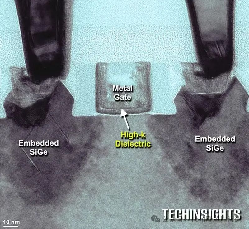
High-k dielectric materials have a higher dielectric constant (k-value) than conventional SiO₂. The types of high-k media are:
|
High-k material |
Dielectric Constant |
|
Hafnium HfO2 oxide |
25 |
|
Titanium oxide TiO2 |
30-80 |
|
Zirconia ZrO2 |
25 |
|
Tantalum pentoxide Ta2O5 |
25-50 |
|
Barium strontium titanate BST |
100-800 |
|
Strontium titanate STO |
230+ |
|
Lead titanate PZT |
400-1500 |
Capacitance Formula: C=ϵ⋅A\d
ε\d is the dielectric constant, AA is the area of the capacitor, and dd is the thickness of the dielectric layer.
As shown in the formula, the larger the ε at a certain C, the smaller the A/d ratio. Even with a high-k dielectric, it is possible to increase the thickness of the dielectric layer while maintaining the capacitance. The physical thickness of high-k materials is more than 3~6 times that of silicon oxide, because the electronic tunneling current is exponentially related to the thickness of the insulation layer, which will significantly reduce the quantum tunneling effect of the gate dielectric layer, thereby effectively improving the gate leakage current.
Send Inquiry