


Why do Advanced Wafer Processes Require FinFETs?
Apr 17, 2025
Leave a message
FinFET technology introduces an innovative three-dimensional transistor structure in wafer fabrication that enables more efficient transistor performance through enhanced gate control and reduced leakage current. This is critical for enabling smaller, faster, and more energy-efficient semiconductor devices. As semiconductor process nodes continue to shrink, the use of FinFET technology is becoming more common and important.
Background: Limitations of traditional planar transistors
In conventional planar MOSFETs, as the process nodes shrink (e.g., from 90nm to 65nm and beyond), we encounter the following technical challenges:
The short channel effect: as the gate length of the transistor decreases, the gate's ability to control the channel decreases, resulting in increased leakage current and reduced switching speed.
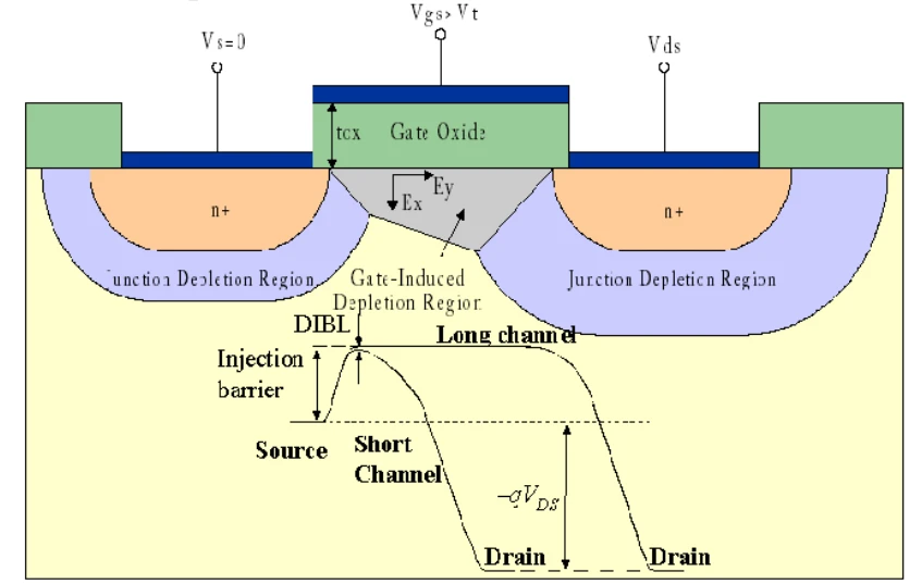
Increased leakage current: An increase in off-state leakage current leads to a significant increase in quiescent power consumption.
Subthreshold Swing Problem: The subthreshold slope of conventional MOSFETs is limited to 60 mV/decade, which limits their switching efficiency at low power operation.
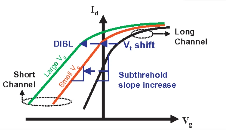
Introduction of FinFET technology
FinFET (FinFET (FinFET) is a three-dimensional transistor technology that improves the performance of traditional MOSFETs by:
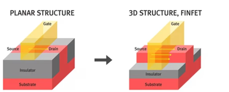
Enhanced Current Drive Capability: FinFETs allow for higher drive currents through a three-dimensional structure. This is because the channel of the FinFET is a "fin" that stands perpendicular to the surface of the substrate, making it possible to achieve a larger effective width in the same footprint.
Better gate control: In FinFETs, the gate can enclose a "fin" channel from three sides, which greatly enhances the gate's ability to control the electric field of the channel, significantly reducing the short channel effect.
Reduced leakage current: FinFETs are able to significantly reduce leakage current through better gate control and shorter effective channel lengths. This is essential for the realization of low-power circuits.
Manufacturing process challenges for FinFETs
Despite the obvious technical advantages of FinFETs, their manufacturing processes also present new challenges:
More complex process flows: Fabricating FinFETs requires more complex process steps, including multiple lithography and etching steps, to form accurate three-dimensional structures.
19-00155-01_aheater Block, 150mm
Equipment and process upgrades: Advanced equipment and processes are required, such as high-precision lithography (EUV lithography) and highly selective etching processes.
Yield control: The complexity of three-dimensional structures increases the likelihood of defects, requiring tighter yield control and inspection techniques.
Verification of the benefits of FinFETsAs
The process moves to the 10nm and sub-nodes, the benefits of FinFET technology become more apparent:
Improved performance and reduced power consumption: With better control and lower leakage current, FinFETs are able to significantly reduce power consumption while maintaining performance.
16-033932-00 6 Inch Showhead Weld
Increased integration: Smaller cell sizes and higher current densities allow chips to integrate more functions and circuitry.
Send Inquiry