


What is PVD-Sputter?
Feb 12, 2026
Leave a message
PVD-Sputter, or sputter coating technology in physical vapor deposition, is a process that uses high-energy particles to bombard a solid target, causing its surface atoms to be knocked out and deposited on the substrate to form a thin film. This technology is widely used in semiconductor, display and other industries for depositing metals, alloys and compound films.
Rationale
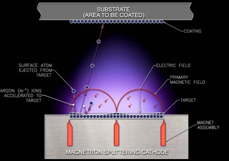
The essence of sputtering is a physical momentum exchange process. Its core principle is to bombard the surface of a target using high-speed moving particles, usually inert gas ions, such as argon ions. Through momentum transfer, the atoms or molecules on the surface of the target gain enough kinetic energy to escape from the surface, fly to the coated part (substrate) and condense into a film.
0040-04745 Chamber Body Hdp-cvd
This process is not local heat evaporation as initially thought, but a collision mechanism similar to "playing billiards". Key evidence supporting this theory includes: atoms sputtered from single crystal targets tend to fly in the direction with the highest crystal density; Sputtering yield (efficiency) is not only related to the energy of the bombardment ion, but also to its mass; And there is an energy threshold below which sputtering cannot occur. Argon (Ar) is the most commonly used working gas due to its content of nearly 1% in air, balancing cost and efficiency.
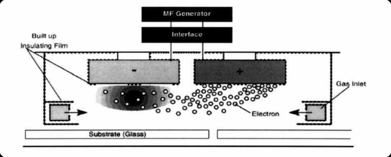
To achieve sputtering, it is first necessary to generate ions that bombard the target. This is usually achieved by gas discharge to create plasma. Under certain air pressure (such as 1~10Pa) and voltage conditions, the gas between the electrodes is ionized to form an electrically neutral gaseous conductor containing electrons and ions, that is, plasma. Among them, the abnormal glow discharge state is specially used for sputtering because of its adjustable current and voltage, which is convenient for controlling the film formation rate and bombardment energy.
Core sputtering technology and its evolution
Depending on the discharge method and electrode structure, sputtering technology has developed into several types.
The most basic DC (diode) sputtering is to use the target as the cathode and the plated part as the anode. The structure is simple, but it has the disadvantages of low film formation rate, increased substrate temperature, high working air pressure, and inability to sputter insulating medium targets. In order to overcome the problem of not being able to sputter insulating targets, RF sputtering was developed, which uses displacement current to pass through the target material by applying high-frequency voltage to achieve sputtering of dielectric materials.
Driven by industrial demand for higher deposition rates, magnetron sputtering has become the mainstream technology. It applies a magnetic field orthogonal to the electric field near the target surface, uses the Lorentz force to constrain electrons, and prolongs their motion path near the target surface, thereby greatly increasing the ionization probability of collision with argon atoms and forming a high-density plasma near the target surface. This significantly increases the sputtering rate and reduces the number of high-energy electrons bombarding the substrate, reducing the temperature rise of the substrate, making it possible to coat heat-resistant substrates such as plastics. Magnetron sputtering sources can operate independently of the plated part and can be used like an evaporation source, extending process flexibility.
In addition, there are technologies such as ion beam sputtering, which uses an independent ion source to generate a high-energy ion beam to directly bombard the target. The particles sputtered by this method have high energy (about tens of electron volts), strong adhesion of the film layer, dense structure, and precise control of process parameters, which are often used in the research field.
Key processes and application areas
A complete set of sputtering equipment and processes involves several key elements. In addition to the target and gas, it is crucial to generate and maintain a stable plasma (Article 2). The process is typically performed in a vacuum environment, where ultra-high vacuum provides a larger average free path of gas molecules and reduces impurity contamination, resulting in better quality films.
In advanced applications such as semiconductor manufacturing, the sputtering process steps are rigorous. Taking the deposition of titanium (Ti)/copper (Cu) films in advanced packaging as an example, the typical process includes: first, high-temperature baking to remove gases (Degas) from the cavity and wafer surface; This is followed by precleaning, which uses argon plasma bombardment to remove the natural oxide layer from the wafer pad to ensure good ohmic contact. Finally, PVD deposition of titanium and copper films is carried out. Parameters such as chamber pressure, air leakage rate, and substrate temperature need to be accurately controlled during the process.
Sputtering technology is indispensable in the field of microelectronics due to its advantages such as wide material adaptability, high film purity, strong bonding with substrate, and good step coverage. In the semiconductor industry, it is used to deposit various metals such as aluminum, titanium, tungsten, tantalum, copper, and their alloy films. In the display industry, such as in TFT array manufacturing, it is used to deposit gates, source-drain electrodes, and ITO (indium tin oxide) transparent conductive films.
PVD-Sputter is a thin film preparation technology based on the principle of physical momentum transfer, which has evolved from DC sputtering to magnetron sputtering, and has become a key process for depositing high-performance metal and compound films in the modern semiconductor and display industries.
END
Send Inquiry