


What are front and rear simulation in IC design?
Feb 10, 2026
Leave a message
Definition and purpose of pre-simulation and post-simulation
Pre-simulation, also known as functional simulation, behavior simulation, or RTL simulation, is mainly performed during the logic design phase, i.e., after the RTL code is completed and before the logic synthesis. The purpose is to verify that the circuit's logic functions in an ideal environment meet design specifications without involving actual physical delays such as gate delays and line delays. Therefore, pre-simulation focuses on the functional correctness of the design, which belongs to the "paper talk" in the early design stage.
Post-simulation is called timing simulation, post-layout routing simulation or dynamic timing simulation, which occurs after the physical design is completed, that is, the end of the layout and routing stage. It is based on a gate-level netlist and a timing file containing actual delay information, taking into account parasitic effects such as device delay, interconnect resistance, capacitance, and inductance. The core goal of post-simulation is to verify whether the circuit can work correctly under real physical constraints, especially whether the timing meets the requirements, which is a "practical exercise" in the later stage of design.
TIN Chamber Assy
The difference between the two in terms of verification content and focus
The pre-simulation mainly focuses on the correctness of circuit functions, focusing on testing whether the logical behaviors such as state machine jumps and data paths are consistent with the design intention. Since the gate delay and line delay are not considered, the simulation speed is fast and logic errors can be efficiently troubleshooted. Its input is an RTL code, which is a behavior-level description and contains no specific physical information.
Post-simulation must further investigate timing compliance and signal integrity on the basis of functional verification. Parasitic parameters introduced by physical design, such as wire resistance, coupling capacitance between adjacent wires, and mutual inductance, can lead to signal delays, crosstalk, voltage fluctuations, and even logic distortion. Therefore, post-simulation needs to be verified in combination with parasitic parameters extracted from the layout to ensure that the signal can be transmitted stably within the specified clock period and avoid chip failure due to timing violations.
Its position and role in the chip design process
From the process point of view, the pre-simulation is in the front-end design stage, usually after the RTL coding is completed and before the logic synthesis. Post-simulation is in the back-end design stage and must be performed after the layout routing is completed and the parasitic parameters are extracted. The layout and wiring determine the specific shape, size and relative position of transistors, metal connections and other devices, and different layout designs will produce different parasitic effects, so they must be verified by post-simulation.
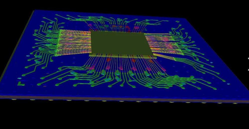
This phased verification method is conducive to risk hierarchical control: pre-simulation can quickly find and correct logical errors to avoid errors flowing into subsequent processes; Post-simulation specifically deals with hidden problems caused by physical effects, such as clock offset and signal crosstalk, to reduce the risk of tape-out failure. If the front imitation is skipped, the back-end adjustment cost will increase significantly; If you skip the imitation, the chip may not work due to actual timing issues.
Simulation tools, efficiency and practical application characteristics
Pre-simulation usually relies on logic verification tools, such as VCS, ModelSim, etc., which have high simulation efficiency and are suitable for large-scale functional testing. Post-simulation needs to rely on the physical design toolchain and is often carried out in conjunction with static timing analysis, which is slow and time-consuming due to the need to simulate the actual circuit behavior.
In actual projects, due to the long time required for post-simulation, all circuits are generally not fully simulated, but are sampled and verified for high-risk paths, such as asynchronous interfaces, multi-cycle paths, etc. In addition, FPGA verification is sometimes seen as an intermediate link between pre-imitation and post-imitation, which can quickly verify functions and partial timing on programmable hardware, but it is still not a complete replacement for post-simulation due to the different physical structures of FPGAs and ASICs.
Pre-simulation and post-simulation each have clear responsibilities in chip verification: the former ensures that the logic is correct, and the latter ensures that the timing is feasible. The two have different inputs, different goals, and different stages, and cannot be combined into a single step. Although the results of the simulation may vary depending on the focus, it is precisely because of this division of labor and cooperation that it is possible to avoid invalid designs from entering the back-end and intercept the final risk before manufacturing, and jointly support the complete verification system from design to realization of the chip.
Send Inquiry