


What are the sources of particles in the semiconductor etching process? and solutions!
Jan 27, 2026
Leave a message
The semiconductor etching process is one of the core links of chip manufacturing, and its accuracy directly determines the performance and yield of chips. As semiconductor technology develops to smaller process nodes, the requirements for etching processes are getting higher and higher, and particle contamination has become one of the key factors affecting etch quality and device performance. Particle contamination can lead to problems such as short circuits, open circuits, and critical dimensional changes, seriously affecting the reliability and stability of chips.
The main source of particle pollution
Equipment source particles
Component wear: Electrodes, gas nozzles, wafer carriers and other components in the reaction chamber are subjected to plasma bombardment and high-speed airflow scouring for a long time, and the surface materials will gradually erode and form metal compound particles.
Internal contamination: Contaminants introduced during equipment installation, maintenance, or use, such as dust, fibers, etc., can interact with materials or reaction products to form particles during the etching process.
Electrostatic suction cup particles: The polymer on the surface of the electrostatic suction cup cannot be expelled, forming rod-like particles that lift and contaminate the wafer when it is released.
2.Process source granules
Chemical Reaction By-products: By-products generated during etching reactions that can form solid particles when reaction conditions fluctuate.
Polymer residue: After plasma etching, polymer residues, micromask by-products, etc. may be converted into particles/residues, which can lead to secondary contamination in subsequent processes if not cleaned properly.
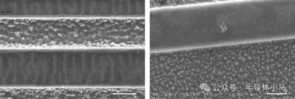
Electrostatic adsorption: The electrostatic field generated by the friction between wafer handling and material enhances particle adsorption, making it easier for particles to be deposited on the surface of the wafer or carrier.
3.Particles of environmental origin
Airborne dust: Dust particles are difficult to completely eliminate, even in a cleanroom environment. When there is a problem with the sealing of the etch equipment FIMS, airborne dust can enter the reaction chamber, interfere with the normal etching reaction and promote particle formation.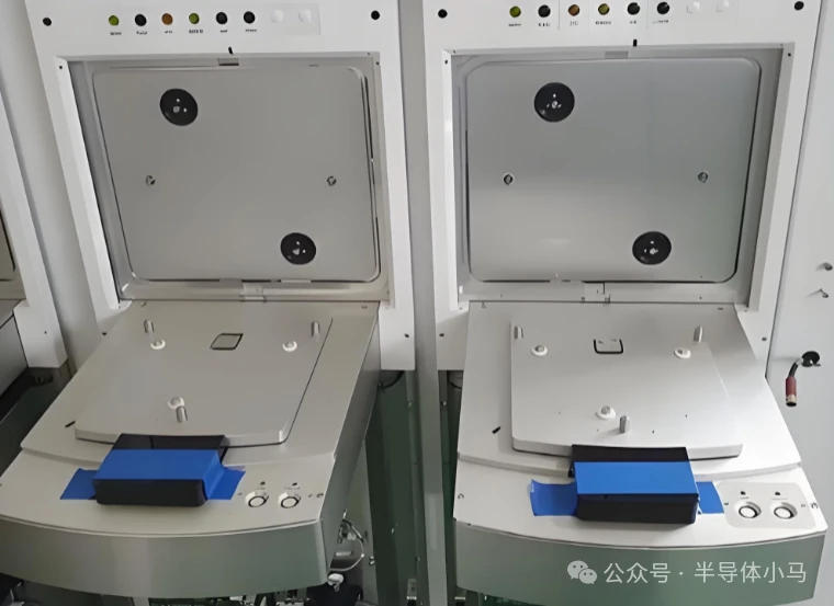
Humidity impact: In a high humidity environment, water molecules may react with etching gases or reaction products, changing the reaction process and product properties, and producing metal chloride particles.
4.Material source particles
Raw material impurities: Even highly purified materials may contain trace impurity elements. For example, metal impurities such as iron, copper, and nickel in silicon wafers can form insoluble compound particles during the etching process.
Post-etching residue: If the reaction products are not discharged from the reaction chamber in a timely and efficient manner, they can accumulate and form particles within the chamber. For example, aluminum fluoride produced during metal aluminum etching can deposit particles on the chamber wall or wafer surface if it is not fully volatilized and extracted.
Solutions to particle pollution
1.Preventive measures
Equipment maintenance: Regularly clean and maintain the equipment, replace worn parts, and ensure that the equipment is well sealed. A waferless automated cleaning (WAC) process is used to remove polymer residue from the inner wall of the chamber.
Process Optimization: Precise control of etching process parameters, such as temperature, pressure, gas flow, etc., to ensure stable reaction conditions. The high-precision temperature control system is used to control the temperature fluctuation within ±0.5°C to reduce the generation of particles caused by temperature changes.
Environmental control: Maintain high cleanliness and appropriate humidity in the cleanroom, and use high-efficiency air filters to remove dust particles from the air.
Control strategy
Static Management: Static elimination equipment is used to reduce static electricity accumulation during wafer handling, reducing the risk of particle adsorption.
Material screening: Select high-purity raw materials to reduce the introduction of impurities. Uses rigorously screened silicon wafers and etching gases.
Process Monitoring: Real-time monitoring of particle generation during etching and timely adjustment of process parameters. The spectral EPD module was used to monitor the fall of particles in the etching chamber.
3.Clearance Scheme
Wet cleaning: A chemical solution is used to remove particles and residues from the wafer surface. For example, diluted hydrofluoric acid (HF) cleaning is used to remove fluoride deposits on the SiO₂/Si₃N₄ sidewall after etching.
Dry cleaning: Uses plasma technology to remove polymer residues and particles from the inner wall of the cavity. For example, inorganic polymers are removed using gases such as fluorinated NF₃, and organic polymers are removed using O₂.
Send Inquiry