


The smaller the chip, the more serious the leakage? What is the leakage barrier reduction effect?
Dec 23, 2025
Leave a message
With the continuous pursuit of thinness and lightness in electronic devices such as smartphones and computers, the size of transistors in chips has been reduced to the nanometer level (such as 3nm and 2nm). However, while the size is shrinking, a physical phenomenon called the "leakage barrier reduction effect (DIBL)" has gradually become a key problem limiting chip performance.
What is the Leakage Barrier Reduction Effect (DIBL)
1.Core definition
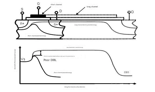
DIBL stands for Drain-Induced Barrier Lowering, which refers to the phenomenon that the potential barrier between the source and the channel is weakened when the drain voltage in the transistor increases. This can cause the transistor to still generate leakage current when it is off, affecting device reliability.
2.Physics mechanism analogy
Imagine a "dam" (barrier) between the source and drain poles, which are normally high enough to block the current (off). However, when the drain voltage increases, it is equivalent to a part of the "dam" being crushed by an external force, and the electrons can "climb" over the barrier to form leakage current.
3.Conditions of occurrence
DIBL is mainly found in short-channel transistors (channel length < 100nm). As the size of the transistor decreases, the interference of the drain electric field on the source electrode increases, making it difficult for traditional device structures to maintain the height of the barrier.
How DIBL affects transistor performance
1.Static power consumption soared
DIBL causes a significant increase in leakage current when the transistor is turned off. According to research, in the 28nm process chip, DIBL contributes more than 30% of the total power consumption. This not only shortens the battery life of the device, but also causes heating problems.
0040-09094 CHAMBER 200mm
2.Threshold voltage drift
The threshold voltage (the critical voltage at which the transistor is turned on) will be offset by DIBL. For example, the threshold voltage of a transistor in a 40nm process may be reduced by 50mV due to DIBL, which directly leads to an increased risk of circuit logic errors.
3.Device life declines
Continuous leakage current accelerates transistor aging. Experiments show that the performance degradation rate of devices with severe DIBL is 2-3 times faster than that of normal devices after working at high temperature for 1000 hours.
How to address the DIBL challenge
1.Material innovation: High dielectric constant (High-k) media
The physical limit of conventional silica (SiO₂) gate media is 1.2 nm (about 5 atoms thick), and further thinning will exacerbate DIBL. Intel introduced hafnium (HfO₂) high-k material at the 45nm node, which increases the dielectric constant by 3 times at the same thickness, effectively suppressing leakage field penetration.
2.Structural Upgrades: FinFET and Full Surround Gate (GAA)
FinFET (FinFET (Fin Field Effect Transistor): By erecting the channel into a "fin" shape and wrapping the gate on three sides, the control of the gate on the channel is increased by more than 50%, significantly reducing DIBL (widely used after the 22nm node).
Nanosheet GAA: Samsung's 3nm process uses multi-layer stacked nanosheets with a gate 360° surrounding the channel, further reducing the leakage caused by DIBL to 1/5 of FinFET.
Process optimization: ultra-shallow junction and strain silicon technology
An ultra-shallow source leakage junction (depth < 20nm) is formed through ion implantation to reduce the lateral interference of the drain electric field on the channel. Strain silicon technology (such as Global Foundries' SiGe channel) is introduced to improve carrier mobility and reduce operating voltage requirements.
Send Inquiry