


Revolutionizing Ion Transport Technology: How HERB™ is Reinventing the Chip Etching Process
Mar 24, 2026
Leave a message
In the sophisticated world of chip manufacturing, the etching process is a critical step that determines the accuracy and performance of circuits. In recent years, breakthroughs in ion transport technology are quietly changing the rules of the game in this field. This article will analyze the evolution of etching processes and their impact on the semiconductor industry by comparing traditional sine wave technology with new HERB™ technology.
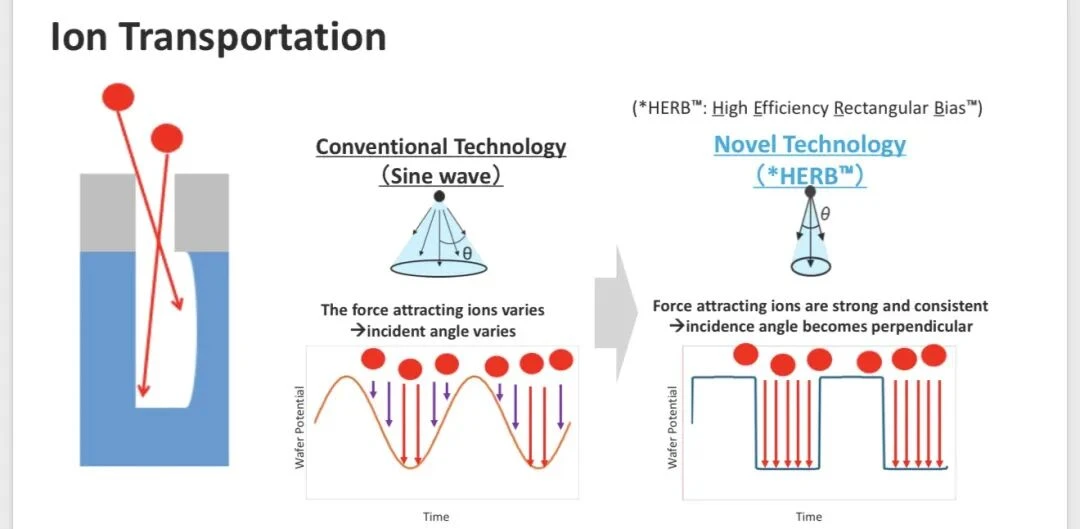
Etching process: the "engraving knife" of chip manufacturing
Chip etching is the process of physically or chemically removing specific materials from the surface of a silicon wafer to form tiny circuit structures. Among them, ion etching technology has become an indispensable link in advanced processes due to its high precision and controllability. The core of ion etching lies in how to precisely and consistently direct ions to the wafer surface.
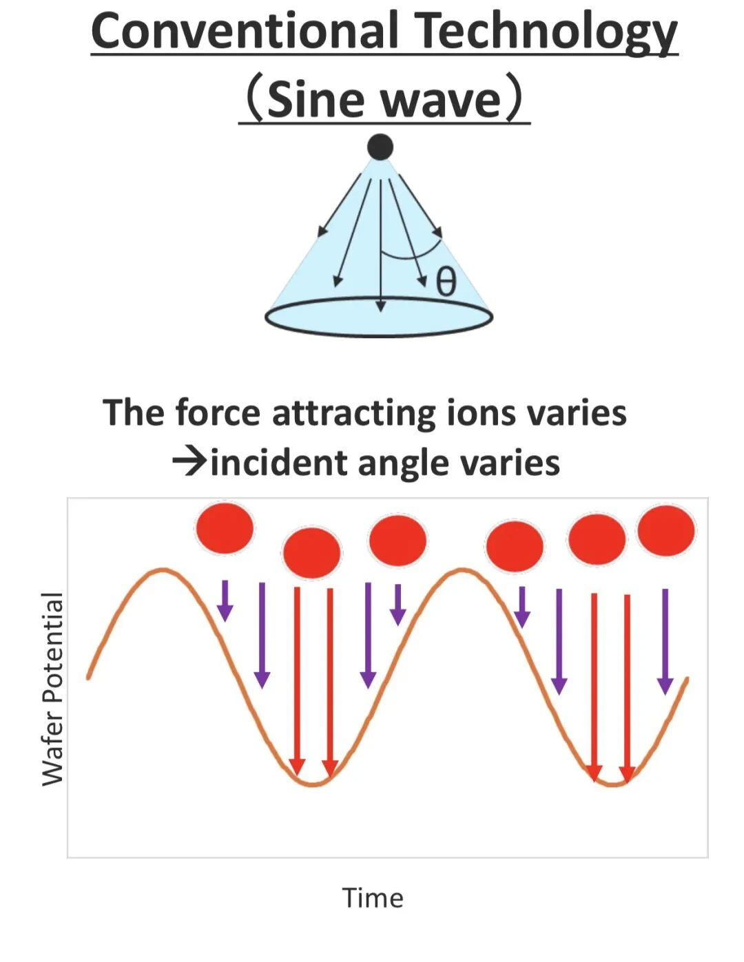
Limitations of traditional technology: sine wave ion transport
Traditional ion etching techniques typically employ sine waves to control ion motion. This model has several inherent limitations: first, the periodic change of the electric field force leads to the constant fluctuation of the attracting ion force and the lack of stability; Second, the ions can hit the wafer surface at a constantly changing angle, resulting in irregular etch profiles; Ultimately, these factors combine to make it difficult to maintain consistent etch depth and sidewall angles in nanoscale processes, limiting process accuracy.
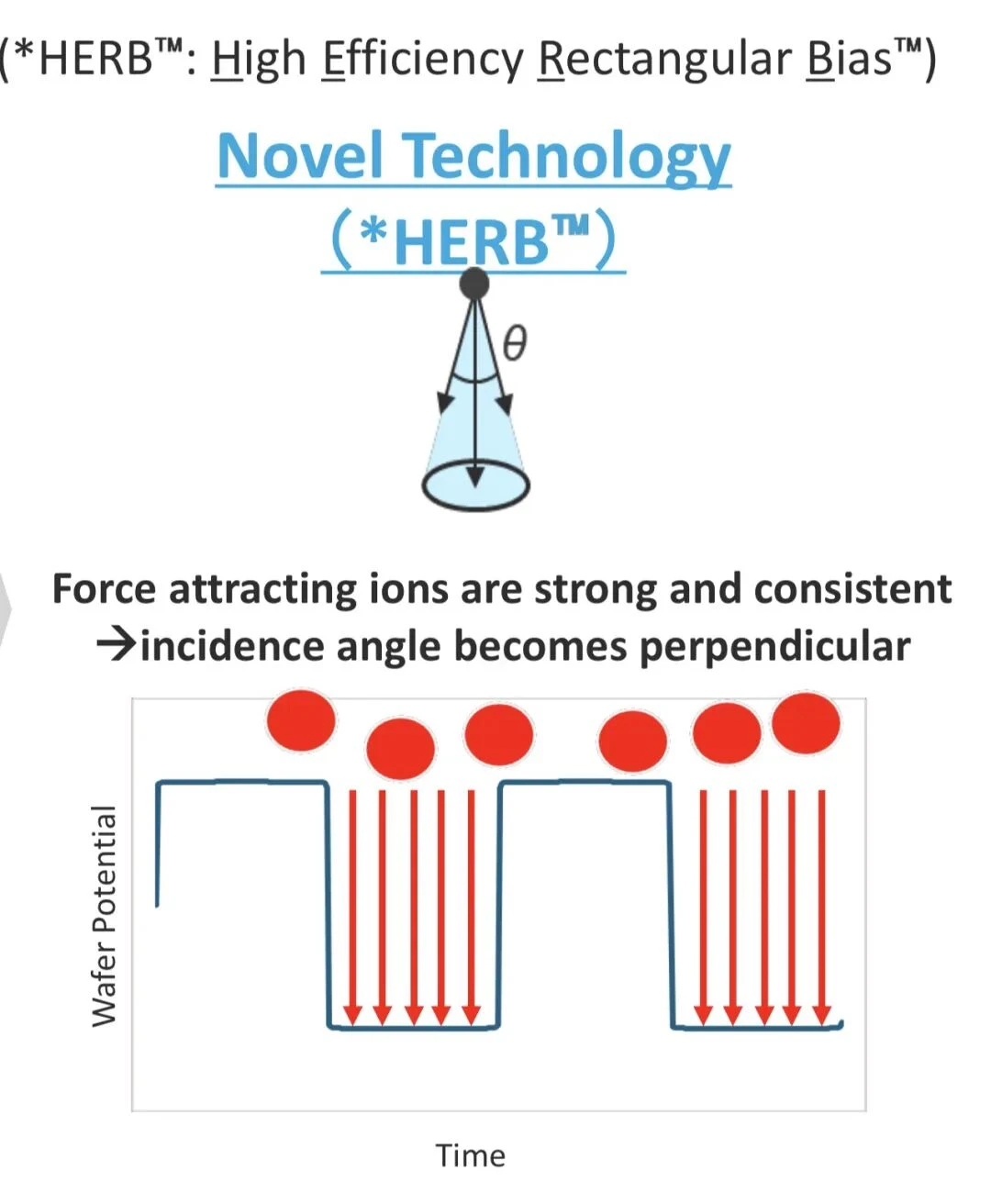
Technological breakthrough: HERB's™ revolutionary ion transport
HERB™ technology represents a significant advancement in the field of ion transport. At its core, it provides a stable and continuous ion guidance force by optimizing the electric field design, allowing ions to strike the wafer surface at a near-vertical angle. This change allows for a more precise and consistent etch profile. At the same time, this technology can maintain the stability of the wafer potential throughout the etching process, significantly reducing process variation.
Practical benefits of HERB™ technology:
HERB™ technology demonstrates multiple advantages in practical applications. It is capable of achieving higher etching accuracy, resulting in more precise etch patterns and steeper and straighter sidewalls. This technology also results in better wafer surface uniformity, allowing for highly consistent etch rates across different regions. These improvements directly translate into improved product yields, reducing chip defects due to uneven etching. What's more, HERB™ technology provides a reliable and efficient etching solution for advanced processes of 3nm and below.
Send Inquiry