


An article to understand the chemical mechanical polishing CMP equipment and process technology
Mar 19, 2026
Leave a message
CMP technology development and principle
Chemical mechanical polishing technology, also known as chemical mechanical planarization, CMP is the most important planarization technology in the manufacturing process of integrated circuits since the 90s of the 20th century.Traditional polishing methods can be divided into two types: chemical polishing and mechanical polishing, chemical polishing has better surface quality, low surface roughness, and shallow damage depth, but the relative polishing speed is very slow and easy to produce fog spots. The damage depth produced by mechanical polishing is deeper, the surface quality is poor but the surface shape accuracy of the processed surface is high, and these two polishing technologies have their advantages and disadvantages.
CMP is a polishing technology that combines the advantages of both, using polishing fluid to chemically react with the workpiece to soften the surface of the workpiece, and then remove the surface reactants of the workpiece through mechanical friction of particles, so that high-efficiency, high-quality polishing and high surface shape accuracy can be performed.
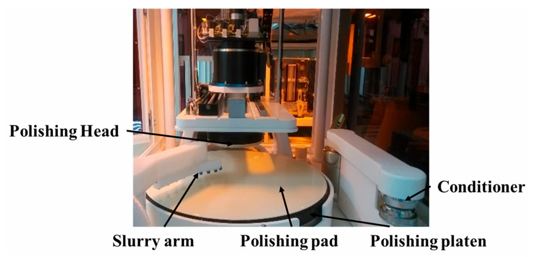
The chemical-mechanical polishing system consists of three parts: a rotating silicon wafer gripper, a rotating table carrying the polishing pad, and a polishing fluid supply device, as shown in the figure below.
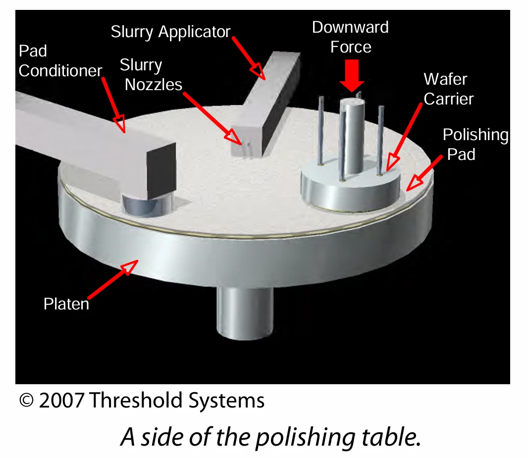
The chemical mechanical polishing process is to make the silicon wafer contact with the elastic polishing pad and make relative motion, and at the same time, the polishing fluid supply system provides acidic or alkaline polishing solution containing abrasive particles, oxidizers, activators, and the surface of the silicon wafer infiltrated in the polishing solution removes the material and flattens under the chemical corrosion of the polishing solution and the mechanical friction interaction of the abrasive particles.
In the process of chemical mechanical polishing, the reaction layer generated by chemical corrosion reduces the strength of the matrix material so that the material mechanical removal can be carried out, and the mechanical action of abrasive particles and polishing pads will continuously expose the processed matrix material, so that the chemical corrosion rate is improved, so that the removal rate of the material is several times higher than that of simple chemical corrosion and mechanical processing.
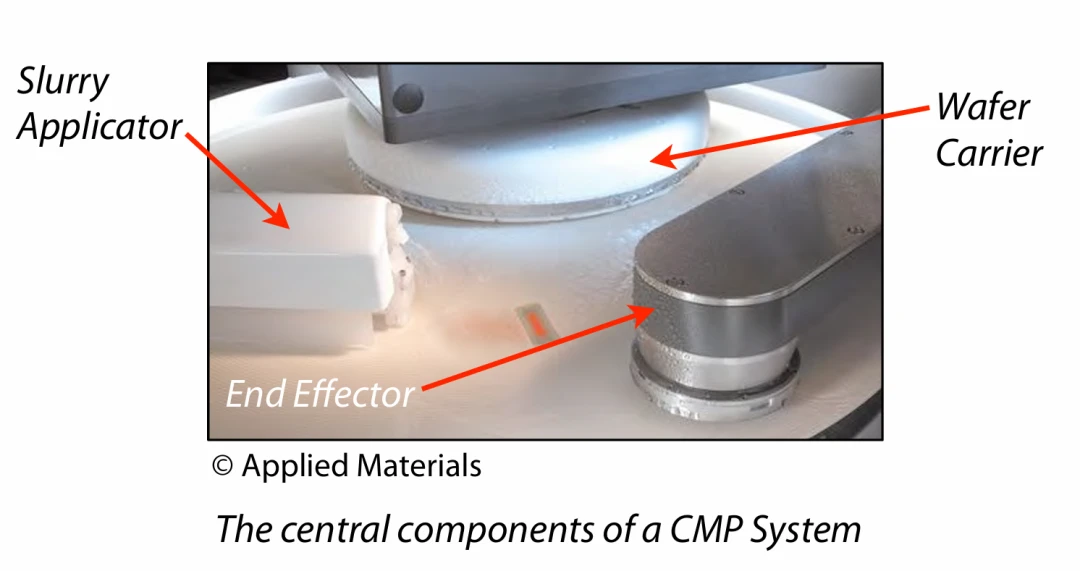
CMP equipment and process parameters
In the process of chemical mechanical polishing, if the mechanical parameters such as speed and pressure are too large, and the mechanical effect in processing is too large, the polished surface of silicon wafers is prone to film peeling, high damage layer and scratch defects, and the material removal rate will also be affected. If the chemical parameters, such as the corrosive ability of the polishing fluid, are prone to corrosion pits, orange peel-like ripples, excessive etching of metal materials, depression of the metal layer, increased roughness and other defects on the polishing surface of silicon wafers. Reasonable adjustment of process parameters to achieve a good match between chemical and mechanical action can obtain high material removal rate and good polishing surface quality.
There are many variables in the CMP process, and its basic process parameter adjustment is mainly to change the speed of the polishing disc, the speed of the gripper and the polishing pressure, the flow rate of polishing liquid, etc. When the rotational speed is very high, the polishing pressure cannot overcome the hydrodynamic force and the silicon wafer will slip. The polishing rate of the wafer will be low and the uniformity will not be well controlled. If the pressure increases, the polishing disc drive system will not be able to overcome the friction to rotate the polishing disc, and the uniformity of material removal on the surface of the silicon wafer will deteriorate with excessive pressure. The Preston equation, which is commonly used as an empirical formula for material removal rates, holds up well in low-speed CMP systems.
Polishing fluid is the main consumable in the process of chemical mechanical polishing, and its performance directly affects the quality of the polished surface. The polishing fluid is mainly composed of abrasive particles, acids or alkalis, ultrapure water and additives, etc., and the ratio of polishing fluid needs to comprehensively consider the removal performance of the material, the corrosion of the slurry on the equipment and the cost of the slurry. For different polished materials, different polishing fluid components are often used. Under normal circumstances, when the abrasive content or particle size in the polishing solution increases, the polishing rate will also increase relatively, and if the increase ratio is too high, it will scratch the surface of the film.
For alkaline polishing fluids, the polishing rate increases as the value increases, but too fast a chemical reaction will reduce the flatness of the polished film. For most CMP processes, the flow rate of polishing fluid is generally 50-125ml/min, usually too small flow rate will lead to unstable polishing rate, too large flow rate will increase process cost and reduce production efficiency. The ultimate goal of polishing fluid research is to find the best combination of chemical and mechanical effects, so as to obtain a polishing solution with high removal rate, good flatness, good film thickness uniformity and high selectivity. In addition, it is necessary to consider issues such as stability, ease of cleaning, corrosiveness to equipment, waste disposal cost and safety.
Polishing pads are another important consumables in the process of chemical mechanical polishing, which are made of polymer materials with holes of 30-50um size, usually polyurethane or polyester saturated polyurethane. The main function of the polishing pad is to deliver the polishing liquid to the polishing area evenly and efficiently, maintain the polishing liquid film on the contact surface, and make the chemical reaction fully carried out. At the same time, the polishing pad is responsible for smoothly discharging the polished reactants and debris to maintain the temperature stability of the polishing area. According to different materials and structures, commonly used polishing pads can be mainly divided into four types: polyurethane polishing pads, non-woven polishing pads, non-woven polishing pads with fluffy structure and composite polishing pads.
The type, compressibility, hardness, density, elastic modulus, porosity, etc. of the polishing pad have a great impact on the polishing quality and polishing rate. The physical and mechanical properties of the polishing pad will affect the surface quality and polishing rate of the processed silicon wafer, and the use of a harder polishing pad can achieve better global flatness and higher intra-wafer uniformity. Using a softer polishing pad allows for better surface quality and improved uniformity inside the chip. Porosity and surface roughness affect the transmission and contact area of the polishing solution, and the rougher the polishing pad, the larger the contact area, the greater the material removal rate, and the increase in porosity. The polishing pad's ability to store polishing fluid is increased, and the material removal rate is increased. The surface of the polishing pad becomes smooth after use, the pores will be blocked, so that the polishing rate decreases, and it must be trimmed to restore its roughness to improve the ability to transfer the polishing fluid.
Introduction to CMP equipment clamping methods
At present, CMP equipment manufacturers generally reduce the non-uniformity of material removal by improving silicon wafer grippers and other measures. As the size of silicon wafers continues to increase, the feature size continues to decrease, and the number of mask layers continues to increase, the focal depth of the lithography machine becomes shorter and shorter, which puts forward higher requirements for the overall situation of each layer. The processing force of chemical mechanical polishing is small, so the adsorption force of the clamping system is not high, but it requires a high flattening ability for silicon wafers. At present, the main clamping methods used in CMP include paraffin bonding, water surface tension adsorption, porous ceramic vacuum suction cup, electrostatic suction cup and film vacuum suction cup adsorption.
Mechanical clamping and paraffin bonding technology: The early silicon wafer fixing methods include mechanical clamps and paraffin bonding, which are easy to warp and deform the silicon wafer or damage the edge area of the silicon wafer, and are rarely used now. The paraffin bonding method is another one of the earlier methods used. The binders and solvents used have a great impact on the cleanliness of silicon wafers, and the binder usually used is paraffin with pine resin as the main component, and organic solvents such as trichloroethylene are used to dewax. For example, when bonding with yellow wax, the silicon wafer is first placed in the fixture to heat, and then the melted yellow wax is infiltrated between the silicon wafer and the fixture, and a certain pressure is applied to make the paraffin stick the silicon wafer to the flat substrate. Filter binders are often melted to remove impurities and ensure reliable wafer bonding. The presence of a bond layer can have an impact on the parallelism and thickness of the silicon wafer. If this method can make the thickness of the paraffin very uniform, it can achieve high polishing accuracy, but the paraffin wax is very time-consuming when peeling and cleaning, and the paraffin must be filtered, so the efficiency is not too high. Moreover, it is not easy to achieve an even distribution of the paraffin layer and to remove the air bubbles contained in the paraffin. (2) Water surface tension adsorption and clamping technology: similar to paraffin bonding, using the tension of water to fix the silicon wafer. The specific method is to glue the mesh foam polyurethane acetate cloth to the surface of the stainless steel substrate, and use the tension of the water on the surface of the foam polyurethane to adsorb the silicon wafer. Guide and position the wafer with a porous baffle and outer circle to prevent the wafer from falling off and sliding during the polishing process. The silicon wafer is placed on the fixture in water and a certain pressure is applied to make the silicon wafer closely bonded to the substrate, and then the fixture is placed in a drying dish until a water molecular film is formed. Then use melted asphalt, paraffin and other oily substances to isolate the silicon wafer for waterproof treatment. The clamping accuracy in this way can reach 0.1um.
Electrostatic suction cup clamping technology: Electrostatic suction cups are mainly used in vacuum environments such as chemical vapor deposition, and can also be used in CMP processing of small-sized silicon wafers. In chemical vapor deposition and dry corrosion processing, vacuum suction cups cannot be used because the processing environment is vacuum. Early mechanical clamping systems used electrostatic suction cups in these processes because they would cause contamination of the wafers and deform during processing due to the contamination of the wafers during processing. The force acting on the suction cup is dispersed, and the silicon wafer will not be deformed on the surface of the suction cup without stress concentration. Wafers can be moved quickly during transportation to improve production efficiency. In the 70s of the last century, electrostatic suction cups were first proposed by Wardly and applied to clamping silicon wafers. Later, due to the many advantages of electrostatic suction cups, many scholars and enterprise research institutions have studied electrostatic suction cups and developed various forms of electrostatic suction cups. It is mainly divided into two categories: one is "flat plate capacitive electrostatic suction cup", the monocrystalline silicon wafer itself is also connected to high voltage, and the other is "integral electrode electrostatic suction cup", which does not directly pressurize the silicon wafer and does not need to energize the silicon wafer, but the adsorption force is small. The distribution of the clamping force of the electrostatic suction cup on the wafer is not fixed. By measuring the distribution of clamping force under different medium thicknesses in the general environment, it is found that the clamping force in the general environment is much lower than that under vacuum conditions. The clamping force of electrostatic suction cups is the smallest among various clamping mechanisms, which is more suitable for clamping small silicon wafers and has a narrow application range.
(4) Vacuum suction cup clamping technology: Vacuum suction cup is the main clamping method of CMP at present, mainly including ordinary porous ceramic vacuum suction cup, vacuum suction cup with rubber part in contact with silicon wafer, piston vacuum suction cup, etc. Piston vacuum suction cups are divided into two types: single-piston and multi-piston. In addition, the vacuum suction cup can be divided into two types: with and without zone pressure adjustment.
CMP application areas
Chemical mechanical polishing technology is widely used in the field of semiconductor manufacturing, such as metal interlayer insulation film, shallow channel isolation, polysilicon, metal, Damascus, etc. flattening, as shown in the figure.
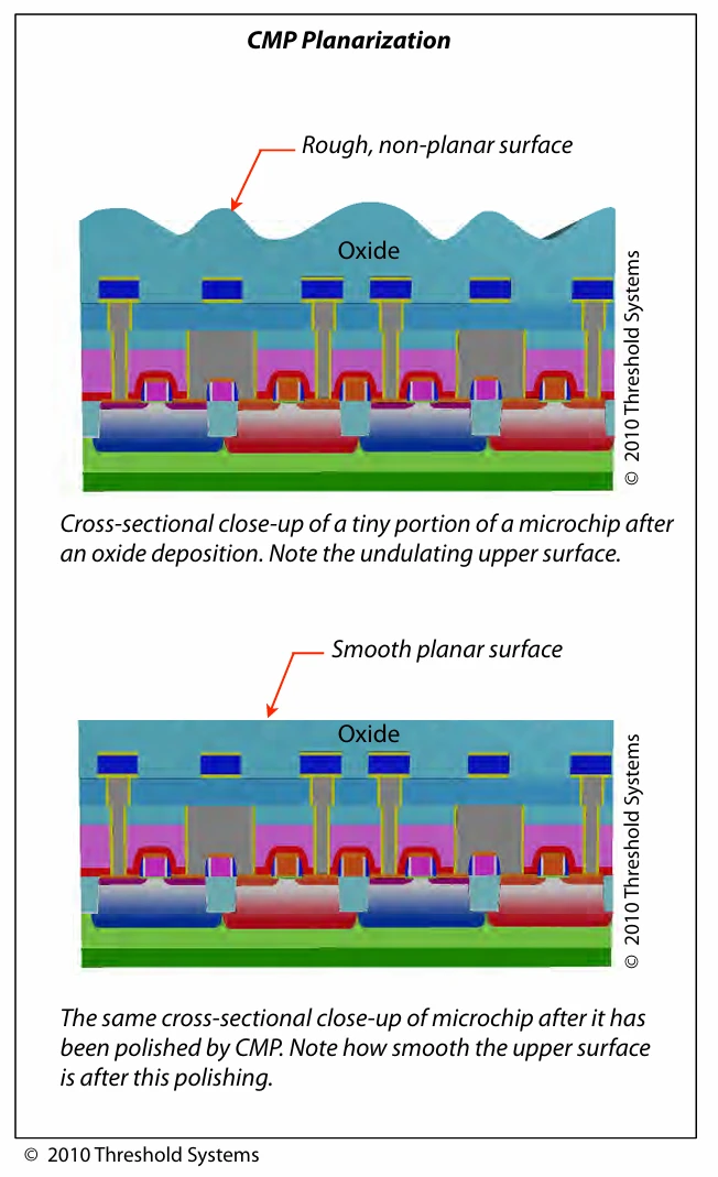
These processes are the most stringent CMP processes, involving a variety of different materials, such as oxides, metals, monocrystalline silicon, polysilicon, etc. In integrated circuit manufacturing, silicon oxide films deposited by CVD method are mostly used for insulating layers or isolation materials. To ensure the flatness of the film layer, excessive deposited material is removed by CMP. The polishing object of shallow channel isolation is mainly the silicon oxide film formed by deposition method in the etching groove, and the silicon oxide film in the trench is the insulating isolation of the circuit in the multi-layer wiring structure, as shown in the figure.
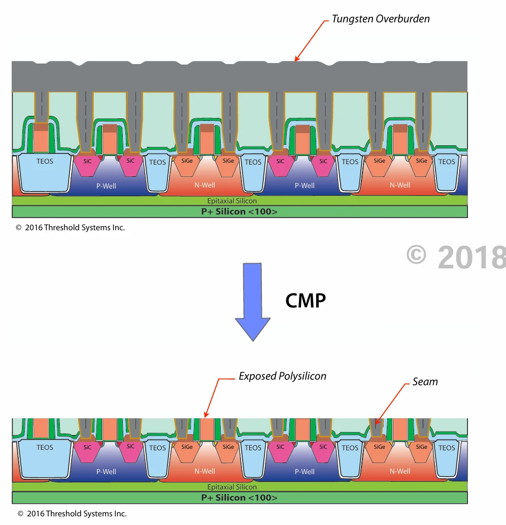
In shallow channel isolation processes, stop layer materials such as silicon nitride are generally required that corrode at a slower rate than silicon oxide films. In the manufacturing process of channel capacitors, the deposited silicon oxide or silicon nitride film is used as the insulating material for the channel capacitor, and the polysilicon is used as the filling material for the channel capacitor, and then the excess polysilicon outside the channel is removed. In wafer manufacturers, CMP is also used in the final step in the preparation of silicon polishing wafers to remove damaged layers and flatten the surface of silicon wafers. In addition, CMP is also used in nickel-aluminum-magnesium phosphide substrates, lenses, thin-film liquid crystal displays, optical glass, conductive glass, ceramics, microelectromechanical system polishing and other products with high surface processing requirements.
Send Inquiry