


Is the Sputtering Target an Anode Material?
Dec 26, 2024
Leave a message
In today's era of rapid development of science and technology, a variety of new materials and technologies are emerging, and sputtering targets, as a key material, play an extremely important role in many fields. However, many people have doubts about whether sputtering targets are anode materials.
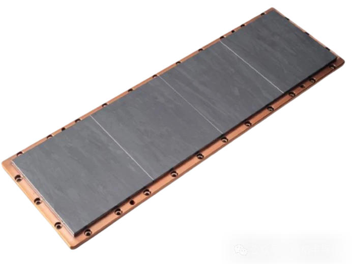
The Basic Concept of Sputtering Targets
Sputtering targets are a widely used material in physical vapor deposition (PVD) technology. To put it simply, it is to sputter out the atoms on the surface of the target by means of ion bombardment and deposit them on the surface of the substrate to form a thin film. These films have a variety of special properties, such as high hardness, good electrical conductivity, excellent optical properties, etc., to meet the needs of different fields.
0010-21827 8" Shield Assy
The Role of Electrodes in the Sputtering Process.
In sputtering equipment, there are usually two electrodes, a cathode and an anode. The sputtering target is generally used as a cathode, as opposed to an anode. When a high voltage is applied between the poles, rarefied gases such as argon are ionized to form plasma. The positive ions are accelerated by the electric field to the sputtering target as the cathode, and the target atoms are sputtered out by collision.
TIN Chamber Assy
The Reason Why the Sputtering Target is not an Anode Material
From the above sputtering process, it is clear that the sputtering target plays the role of cathode, not anode. The main reasons for this are:
Ion bombardment object: The core principle of sputtering is to use ions to bombard the target to make the target atoms escape. Under the action of the electric field, the positive ions move towards the cathode (i.e., the sputtering target) and collide, which determines the cathode properties of the sputtering target in the sputtering system.
2. Material properties and functions: The sputtering target is mainly selected based on the type of deposited atoms it can provide and its own physical and chemical properties, such as purity, density, crystal structure, etc., which are fundamentally different from the functional requirements of anode materials in the sputtering process.
A wide range of applications for sputtering targets
1.Semiconductor industry: In the chip manufacturing process, sputtering targets are used to deposit various metal films, such as copper and aluminum, as circuit connection layers or barrier layers, which play a key role in the performance and reliability of chips.
2. Flat panel display industry: Transparent conductive electrodes (such as indium tin oxide, ITO) and various metal electrode films used in the manufacture of liquid crystal displays (LCDs) and organic light-emitting diode displays (OLEDs) ensure the characteristics of high definition, high brightness and low power consumption of displays.
3. Solar photovoltaic field: It can be used to deposit battery electrodes and anti-reflective coatings, etc., to improve the photoelectric conversion efficiency of solar cells and promote the development of clean energy.
In summary, the sputtering target is not an anode material, but acts as a cathode during sputtering, providing an atomic source for thin film deposition by ion bombardment. Its outstanding performance in semiconductors, flat panel displays, solar photovoltaics, and many other fields underscores its importance as a key material. With the continuous progress of science and technology, the research and development and application of sputtering targets will continue to deepen, and contribute more to the innovation and development of various industries.
Send Inquiry