


Introduction to wafer foundry
Jan 20, 2026
Leave a message
Foundry refers to a business model that specializes in semiconductor wafer manufacturing and accepts commissions from other integrated circuit (IC) design companies without engaging in design. It is one of the important links in the semiconductor industry, with the characteristics of technology-intensive, capital-intensive and connecting the previous and the next.
The basic concepts and models of wafer foundry
The business models of integrated circuit manufacturing enterprises mainly include IDM mode and wafer foundry model. The IDM (Integrated Device Manufacturer) model refers to a vertically integrated semiconductor company that handles everything from design, manufacturing, packaging and testing to the sale of its own brand ICs, and early companies such as Intel, Texas Instruments, Motorola, IBM and other companies all adopted this model.
Wafer foundry refers to a semiconductor industry business model that accepts the commission of other fabless design enterprises (Fabless) and specializes in the processing and manufacture of integrated circuits of wafer finished products, and does not engage in product design and back-end sales on its own. This model originates from the specialized division of labor in the integrated circuit industry chain, forming three major links: fabless design enterprises, wafer foundry enterprises, and packaging and testing enterprises.
0020-27113 CLAMP RING 6 SMF TI
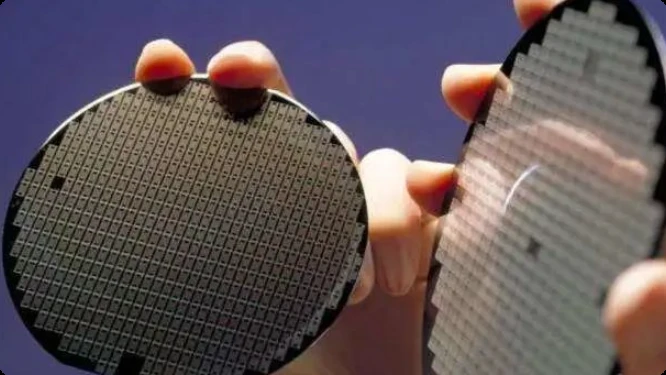
In foundry, the foundry is responsible for the entire wafer manufacturing process, including sourcing raw materials, growing wafers, cutting, cleaning, film deposition, and subsequent packaging and testing steps. This allows chip design companies or brands to focus on key areas such as product design, marketing, and R&D, and entrust the manufacturing process to professional foundries, thereby saving money and resources, reducing production costs and risks, and being more flexible and agile in market competition.
The location of the foundry industry chain
The upstream of the industrial chain of the wafer foundry industry provides semiconductor materials, equipment and related design services, mainly including semiconductor materials such as silicon wafers, photoresists, mask plates, electronic special gases, sputtering targets, lithography machines, etching machines, ion implanters, gluing and development equipment, thin film deposition equipment and other semiconductor equipment, as well as IC design services.
The midstream of the industrial chain is the wafer foundry processing service link, and its process includes wafer cleaning, lithography, etching, ion implantation, annealing, diffusion, chemical vapor deposition, chemical mechanical grinding and other steps. Representative wafer foundry manufacturers on the market include TSMC, Globalfoundry, SMIC, Hua Hong Group, VIS, PSMC, Jinghe Integration, etc.
The downstream of the industrial chain is wafer packaging and testing, as well as wafer terminal applications such as consumer electronics, semiconductors, photovoltaic cells, and industrial electronics.
The development history of wafer foundry
1970s-1980s: Integrated Design and Manufacturing (IDM) Era. In the early days, the semiconductor industry implemented the IDM model, that is, chip design, manufacturing, packaging and testing one-stop self-operation. Due to the high cost of manufacturing equipment and extremely high technical thresholds, small companies basically do not have the ability to enter the manufacturing process, and the chip industry is dominated by large companies.
Mid-1980s: The foundry model was born. In 1987, Taiwan Semiconductor Manufacturing Co., Ltd. (TSMC) was founded by Zhang Zhongmou in Taiwan, China, creating a pure manufacturing, design-free foundry business model, breaking the situation of IDM dominating the world for the first time.
1990s: Foundry takes off. TSMC has rapidly expanded production and improved its process capabilities, becoming the world's leading foundry. UMC has also transformed into a professional foundry in Taiwan. In the United States, Chartered Semiconductor (later merged into Globalfound) appeared. At the same time, a large number of Fabless companies have emerged, promoting the explosive growth of mobile communications and consumer electronics, and the "Fabless + Foundry" model has become the new mainstream.
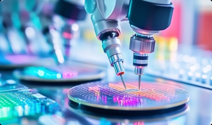
2020s to present: advanced processes, geopolitics and global layout. The industry has entered the 3nm era, and TSMC, Samsung, and Intel (returning to the foundry market and establishing IFS) have started a head-to-head confrontation. Geopolitical tensions (such as the Sino-US technology war) have prompted wafer foundry production capacity to begin to be deployed in many places around the world, such as TSMC setting up factories in the United States and Japan, Samsung investing in Texas, and SMIC accelerating its expansion in Chinese mainland.
Emerging fields such as automotive electronics, AI chips, and the Internet of Things have put forward more segmented needs for wafer foundry, and mature processes (such as 28nm and 40nm) have also become key competitive areas, especially in the automotive and industrial fields.
Process classification and market status
The wafer manufacturing process can be roughly divided into advanced logic process and characteristic process. According to the process, it can be divided into advanced process and mature process, generally below 14nm is called advanced process, and 28nm and above is called mature process.
As process nodes evolve, the investment in the required equipment increases significantly. The equipment investment required for special processes (generally 40nm and above) is US$2 to 3 billion per 50,000 wafer production capacity, while the investment required for advanced processes (28nm and below) is at least US$4 billion.
At present, the global wafer foundry industry presents a competitive pattern of "one super and many strong". TSMC, as an industry leader, occupies about 60% of the market share. From the perspective of geographical distribution, by 2027, Chinese mainland is expected to dominate the field of mature processes, while advanced processes are still dominated by Taiwan, China.
According to SEMI data, rising chip demand has led to continuous growth in global semiconductor fab production capacity, which will increase from 31.5 million pieces/month in 2024 to 33.7 million pieces/month in 2025 (calculated as 8-inch wafer equivalent), with growth rates of 6% and 7%, respectively. Global semiconductor sales are expected to grow at a compound annual growth rate of 9% between 2025 and 2030, totaling more than $1 trillion by 2030.
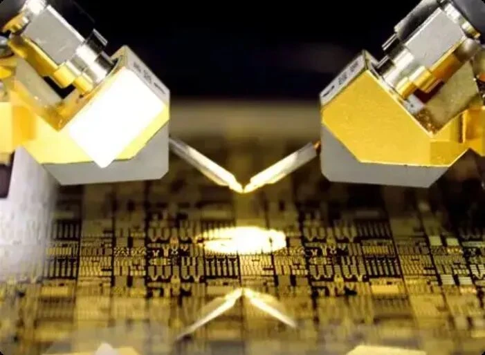
Mainly involved in enterprise and technology trends
At present, the main companies participating in wafer foundry in Chinese mainland include SMIC, Hua Hong Semiconductor, Jinghe Integration, Xinlian Integration, etc. SMIC is one of the world's leading integrated circuit wafer foundries and a leader in the integrated circuit manufacturing industry in Chinese mainland. Hua Hong Semiconductor is the world's leading characteristic process wafer foundry enterprise, and it is also one of the enterprises with the most comprehensive coverage of characteristic process platforms in the industry; Jinghe Integration ranks first in the global market share in the field of LCD panel driver chip foundry; Xinlian Integration focuses on technology platforms such as power devices, MEMS, BCD, MCU, etc., and the AI field has become its new growth point.
Taking TSMC as an example, the development trend of wafer foundry technology is as follows: global production capacity continues to expand, market share is concentrated in leading enterprises; The 3/2nm process dominates the high-end market, the advanced process is accelerating, and the competition for mature processes is fierce. Packaging and process technology will develop in tandem, and the 2nm process will be based on GAAFET. With the development of AI, the demand for high-performance computing (HPC) continues to expand, further driving the demand for wafer foundry.
Wafer foundry work is the core link of the semiconductor industry, allowing design companies to focus on innovation through specialized division of labor, while manufacturing companies continue to promote process evolution and capacity expansion. At present, driven by emerging demands such as AI, automotive electronics, and the Internet of Things, advanced processes and characteristic processes have ushered in important development opportunities, but they also face multiple challenges such as geopolitics, supply chain dependence, and technology yield. In the future, the global foundry industry will continue to evolve in technology competition and production capacity layout.
Send Inquiry