


3D NAND Process
Oct 16, 2024
Leave a message
TIN Chamber Assy
3D NAND Process
In today's digital age, the demand for data storage is increasing, and the performance requirements for storage devices are also increasing. As an advanced non-volatile storage technology, 3D NAND has been widely used in mobile devices, personal computers, and even data centers due to its high density, large capacity, and long life. This article will briefly introduce the manufacturing process of 3D NAND.
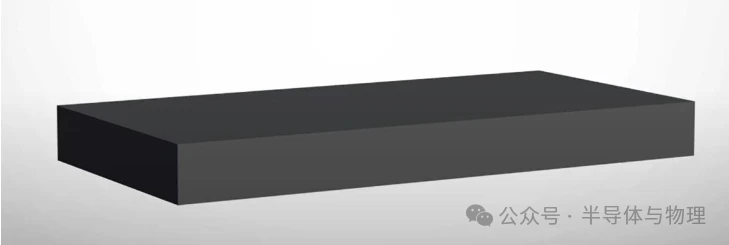
Silicon wafers with a specific crystal orientation are selected as the substrate
The fabrication of 3D NAND begins with the selection of a high-quality monocrystalline silicon wafer with a specific crystal orientation, such as < 100 > or < 110 >. Choosing the right wafer orientation is critical for subsequent process steps, as it directly affects the performance and reliability of the transistor.
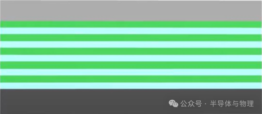
CVD is used to alternately deposit multi-layer thin films
Next, chemical vapor deposition (CVD) is used to alternately deposit multiple layers on a silicon substrate until the desired number of layers is reached. The two most common material combinations are oxide-nitride and oxide-polysilicon, with Samsung choosing silicon nitride and silica as the material system for its 3D NAND products. The challenge of this process is to ensure that films with high stack counts have precise thickness and good uniformity, which is critical to maintaining the consistency and reliability of device performance.

A hard mask for deposition channel etching
In order to achieve the subsequent fine patterning, a hard mask needs to be deposited on top of the multilayer film, which is usually an amorphous carbon film with high etching resistance. This mask layer will protect the parts that do not need to be etched and guide the subsequent trench etching process. The gases used in the etching process are mainly oxygen (O2), supplemented by nitrogen (N2) and hydrogen (H2) to optimize the etching effect.
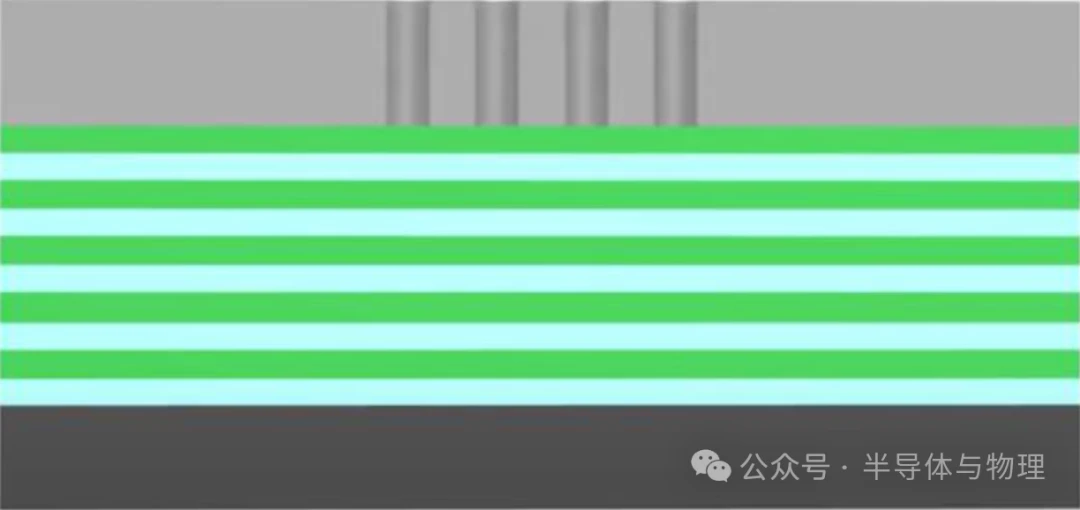
The hard mask is opened by etching
After the area to be etched is defined using photolithography on the hard mask, the hard mask at the specified position is removed by dry etching, exposing the multilayer film underneath. This step is key to accurately controlling the size and shape of the device.
Trench through hole etching
Next, the channel vias are etched using fluorine-containing gases such as SF6 or CF4, a process that requires very high precision to ensure that each through hole accurately penetrates all layers to reach the silicon substrate at the bottom.

Step etching
Subsequently, step etching is carried out, which is treated with different gas combinations for silicon oxide (e.g., CF4/CHF3) and nitride (e.g., CH2F2), respectively, to form the desired structure.

Slit etching
Slit etching is used to further refine the structure in preparation for the formation of the character line later. This process also requires a high degree of precision and control.
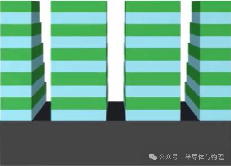
Etching SiNx to form a character line
After slit etching, silicon nitride (SiNx) is etched using a specific process to form a character line, which is an important part of connecting the individual memory cells.
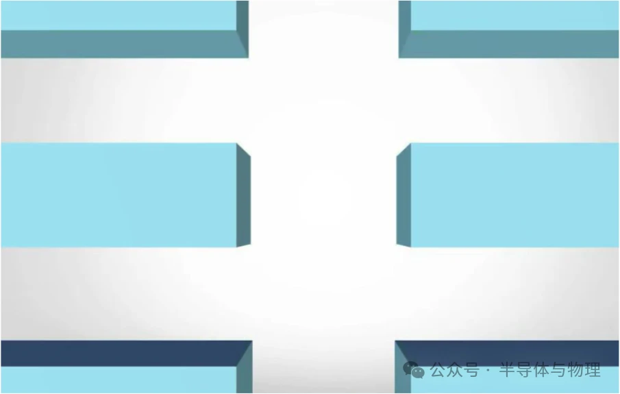
Word line filling and channel through hole filling
After the lines are formed, they are sequentially filled with conductive materials such as titanium nitride (TiN) and tungsten (W) to achieve a good electrical connection. At the same time, the channel vias need to be filled to ensure that each memory cell can be effectively connected to the external circuitry.
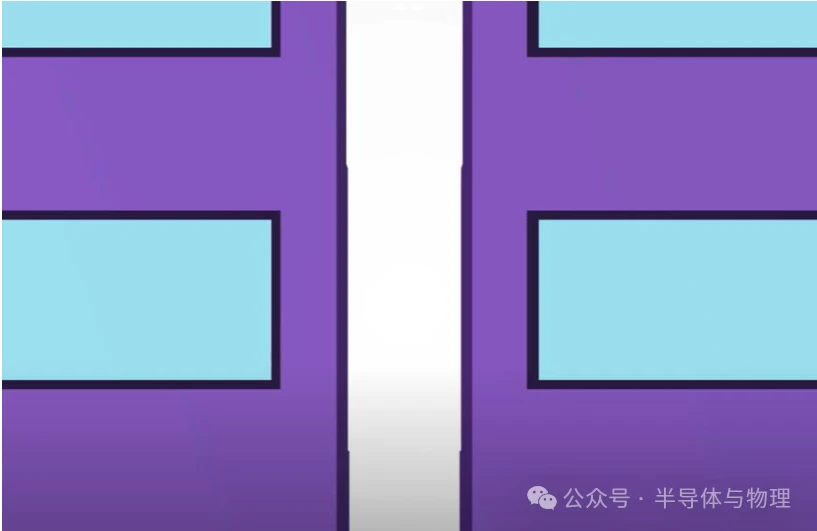
Channel through-hole filling
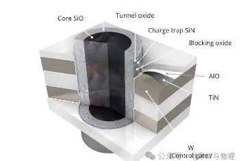
It is filled with a variety of materials, including gate oxide, floating gate, tunneling oxide, active polysilicon, and central SiO.
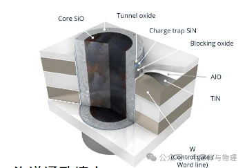
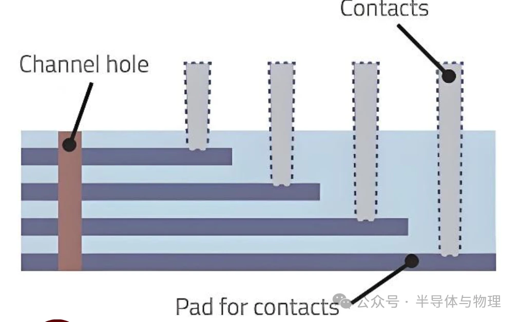
Contact hole etching
Etching of the contact holes is carried out to establish the connection from the top metal layer to the storage cell. Etching of contact holes also requires high precision and control.
Contact hole filling
Finally, the contact holes are filled with conductive materials such as aluminum or copper, ensuring low resistance and stable electrical properties.
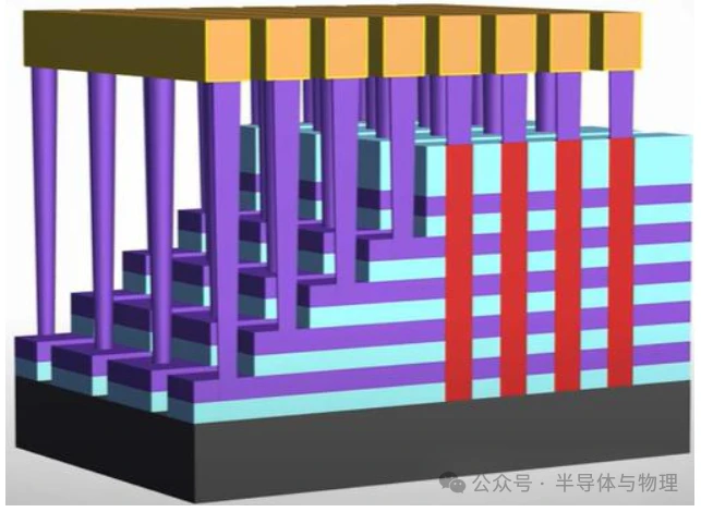
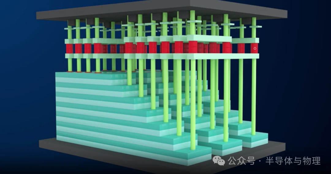
The fabrication of 3D NAND is a complex and sophisticated process that involves several critical steps and technologies. With the continuous advancement of technology, 3D NAND is expected to achieve higher storage density, faster data read and write speeds, and lower energy consumption in the future, and continue to promote the development of information storage technology.
Send Inquiry