


What is SK Hynix's newly released iHBM technology?
Jun 11, 2026
Leave a message
With the continued growth in demand for artificial intelligence and high-performance computing, high-bandwidth memory (HBM), as a high-performance DRAM based on 3D stacking technology, has become a core storage component in modern AI data centers. To improve performance, chip manufacturers are constantly increasing the number of HBM stacking layers, accelerating from the mainstream 12 or 16 layers to more than 20 layers. However, this process has led to a sharp increase in power consumption and heat generation, making heat dissipation a key bottleneck restricting the performance release of next-generation AI chips.
As NVIDIA's Blackwell architecture GPUs break through the kilowatt barrier in power consumption and the number of HBM stacked layers approaches 16, effectively controlling the power density of the D2D PHY (Die-to-Die Physical Layer, the physical interconnect channel that enables ultra-high-speed data transmission between the HBM base chip and the AI high-speed chip) region connecting the HBM and the GPU is becoming the core of the competitiveness of next-generation HBM technology. Heat dissipation is no longer a bonus, but a key factor determining whether the chip can operate stably and maintain its yield rate.
Core Innovation
On May 26, 2026, SK Hynix officially released its "iHBM" technology (integrated cooling High Bandwidth Memory) . This technology significantly reduces heat generation during product operation by integrating an integrated cooling element (ICE) within the HBM package.
Traditional HBM relies on indirect heat dissipation through the core die, which is a long and difficult process that causes heat to accumulate in the center of the chip. iHBM technology fundamentally solves this problem at the structural level by embedding an ICE (Insulated Component for Heat Dissipation) directly within the D2D PHY region where heat is most concentrated. An ICE is a component made of insulating, highly thermally conductive silicon-based material that can create a dedicated heat path inside the HBM package.
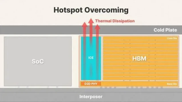
According to official test data, compared to traditional solutions, iHBM can reduce thermal resistance by more than 30% while ensuring stable operation of the product under high temperature and high load conditions. This means that in demanding AI training environments, memory chips equipped with this technology can maintain good operational stability and reduce computing power fluctuations caused by overheating.
Advantages in process and compatibility
In terms of mass production capabilities, iHBM will utilize the market-proven advanced MR-MUF (Match Reflow Molding Underfill) wafer-level packaging process, enabling stable, large-scale mass production. Furthermore, SK Hynix stated that this technology boasts high design compatibility with customers' existing SiP (System-in-Package) environments. For downstream customers like NVIDIA and AMD, replacing memory chips typically requires redesigning the GPU substrate or adjusting the packaging mold, resulting in high costs and impacting product iteration cycles. iHBM, however, can be deployed directly without large-scale design modifications, effectively lowering the barrier to entry for this new technology and facilitating its rapid adoption.
SK Hynix plans to apply iHBM technology to next-generation products such as HBM5 to meet the stringent thermal management requirements of highly integrated and high-bandwidth applications such as high-performance computing (HPC) and AI data centers, thereby further improving the stability and operating efficiency of the overall system.
Industry Exploration and Strategic Significance
Looking at the market, iHBM is not the first technology to attempt to integrate heat dissipation capabilities into the chip itself. Samsung Electronics is developing a "multi-layer stacked FOWLP" technology that combines ultra-high aspect ratio copper pillars and fan-out wafer-level packaging (FOWLP). Its Exynos 2600 chip uses HPB cooling technology, which can be directly packaged on the chip along with the DRAM. Microsoft has also developed "microfluidic cooling technology," which delivers coolant into the chip through tiny channels. Furthermore, the industry is exploring heat dissipation solutions that combine diamond as a substrate material with copper, potentially leading to significant improvements in heat dissipation performance.
Currently, chip heat dissipation technology is evolving from single external cooling solutions such as air cooling and liquid cooling towards a synergistic approach of optimizing internal packaging materials, improving structure, and integrating external cooling. The next round of technological competition among the three major memory giants-SK Hynix, Samsung, and Micron-has shifted from the number of stacked layers and transmission speed to integrated cooling and power density. For AI infrastructure, advanced heat dissipation technology is a prerequisite for unlocking next-generation storage performance and directly impacts data center operating costs-HBM failures are one of the leading causes of GPU failures in data centers. Lowering operating temperatures not only reduces hardware damage and downtime maintenance costs but also prevents computing power throttling caused by triggering temperature control thresholds .
Send Inquiry