


NAND Flash Introductrion-2D NANDArray
Feb 04, 2026
Leave a message
1. Review: Single transistor structure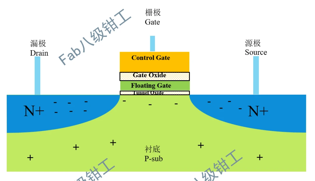
The formation of a string
Let's start with the most basic unit, the formation of strings, also known as strings. First, let several floating gate transistors hold hands (here are four examples):
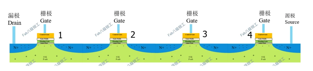
After the floating gate transistor is held in hand, the four transistors share a substrate; Each has its own gate.
At this time, if you want to complete the erasure, you can complete the erasure of all four floating gate transistors by adding a high voltage such as 20V to the substrate. If you want to complete the write, you need to increase the voltage on the floating gate transistor that needs to be written, such as 20V. And if you need to complete the reading, it is a similar process. If the four floating gate transistors are SLC spec, 0100 is now required
Step 1, erase
The substrate is connected to 20V, and the floating gate transistor gate is applied with low voltage to suck all the charge out of the floating gate and maintain a charge-free state.
The second step is to write
· 0=There is a charge in the floating grid
· 1=No charge in the floating grid
To write 0100, the corresponding state is: Charged - No Charge - Charged - Charged
Therefore, the high voltage is given to the three floating gate transistors 1, 3, and 4, such as 20V, and there is no charge in the floating gate transistor No. 2, so the threshold voltage Vth is 5V, and the source drain at both ends is connected to a low level, and 0100 can be written.
It should be noted that the source and drain are connected to low voltage to prevent the channel effect. If a high voltage is applied to the drain, a channel effect will be formed, affecting electrons being attracted into the channel by the gate, i.e., affecting the write.
Step 3, read
As mentioned earlier, after the charge is stored in the floating gate, the original threshold voltage Vth cannot generate a channel due to the cancellation effect caused by the charge in the floating gate. Therefore, the voltage needs to be increased to generate the channel.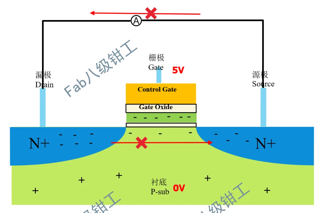
When the charge is stored, the opening voltage of the floating gate transistor increases. Assuming that choosing 10V can ensure that the floating gate transistor will not tunnel or conduct. Under this condition, a transistor is read separately, taking the No. 1 floating gate transistor as an example:
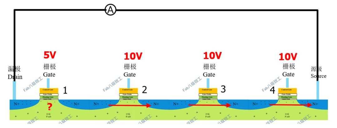
The drain increases the voltage. The gate of No. 2, 3, and 4 plus 10V, this voltage can generate a channel regardless of whether a charge is stored or not, and it can be regarded as a conductor. Transistor No. 1 adds Vth=5V to read the current Id. If the Id is detected, the No. 1 transistor is considered to be in a state-free charge-free storage state, and if the No. 1 transistor has a charge, it cannot be turned on, and the Id is very small and can be ignored.
Read transistors 1, 2, 3, and 4 in turn to get 0100. If it is a larger capacity such as MLC, it is necessary to increase the voltage sweep. Next, a 2D NAND array is formed. For 2D arrays, there are two dimensions, X and Y, that is, multiple Strings. Each string has multiple floating gate transistors.
At this time, you need to add a strobe at each end, that is, an ordinary MOS tube, as a switch to select a specific string. Strobe tubes are divided into SGS (Select Gate Source) and Drain Strobe SGD (Select Gate Drain).
The basic string of 2D NAND is constructed as follows (taking 4 floating gate transistors as an example):

有了基本串,我们进行阵列排列,将每个横排浮栅晶体管和选通晶体管的栅极分别连起来.
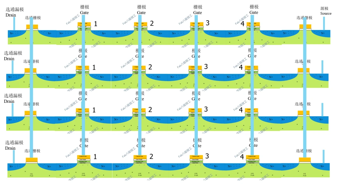
In order to simplify, the following is no longer represented by the color diagram of the MOS tube, and the simplified model is adopted. The MOS tube has only one gate, as shown in the diagram below:

Floating gate transistors have two gates, as shown in the diagram below:

So there is the following array:
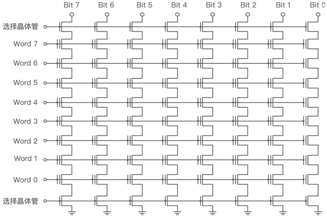
Each String connects a Bit Line, called a bit line. The floating grids of each line are connected together on a word line, called a word line. All floating gate transistors connected on the same word line form a page. The above is just a simple schematic, usually in the actual NAND chip, there can be tens of thousands of word lines and bit lines in total. As arrays grow in size, they need to be grouped at different levels. For example, in order to facilitate the management of residents, our city is also managed according to the levels of province, city, district, county, street and community. Similarly, NAND arrays have such a concept. The smallest cell is called a cell, which is a floating gate transistor.
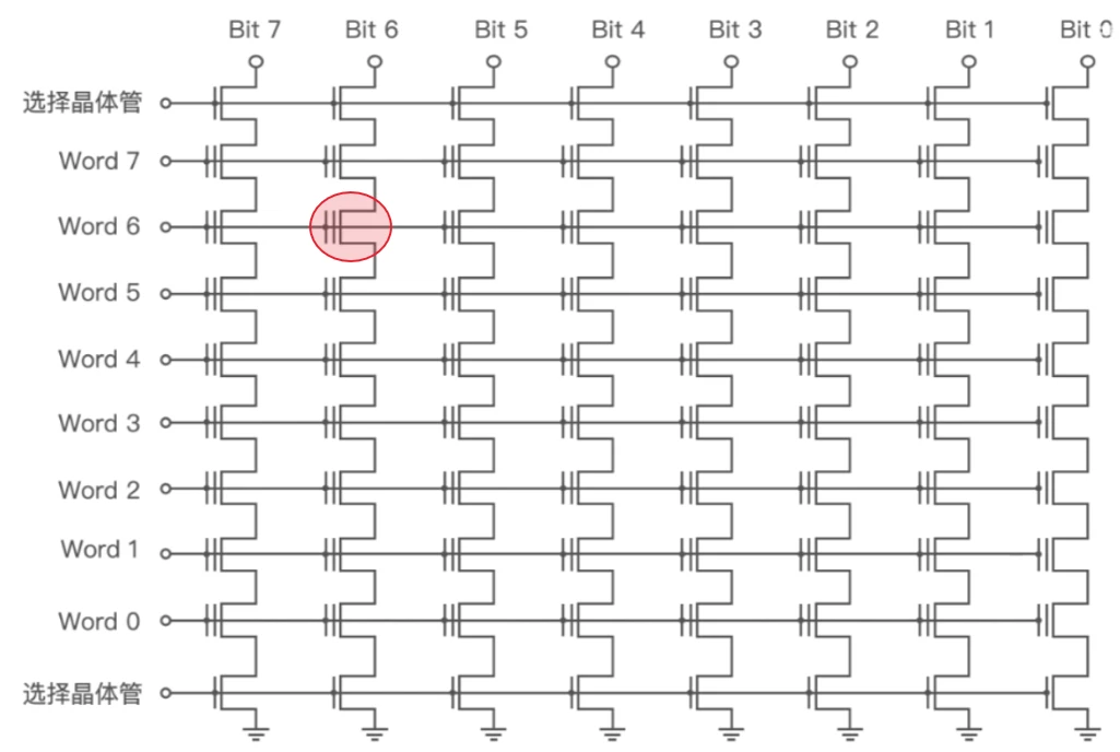
The second is String, the smallest series unit, usually tens to hundreds of cells connected in series, and each end has a strobe MOS tube.
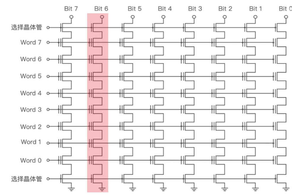
Then there is the Page page, which is the smallest writing unit, that is, all the cells connected to the Word Line form the page.
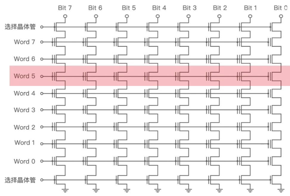
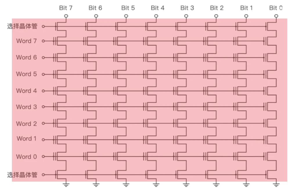
If the floating gate transistors in the figure are connected to a substrate, a single block can be erased by increasing the voltage on the substrate, and such a basic unit is called Block. That is, the smallest erase unit.
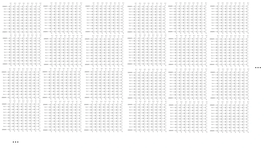
As the array continues to expand, many blocks will be in the same plane, also known as a plane.
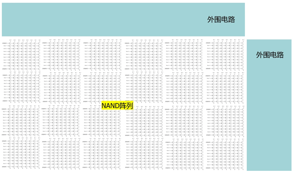
In the era of 3D NAND, from bungalows to buildings, Slit isolation slots were created to isolate planes and blocks. In addition, NAND storage is not just a storage array, but also needs to set up peripheral circuits in the peripheral area for address compilation and logic operations. The peripheral circuit is called the Peripheral zone. In the 2D era, peripheral circuits are distributed around the periphery of the array.
Send Inquiry