


An article to understand the manufacturing method of microchips
Apr 28, 2026
Leave a message
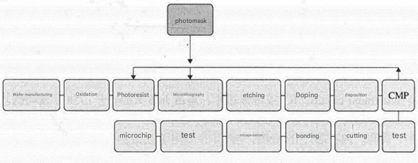
As the core pillar of the semiconductor industry, microchip manufacturing continues to break through physical limits in its process complexity and technical precision, and is accelerating its evolution towards sub-3nm processes, 3D integration and green manufacturing. As a basic material, silicon has become an ideal carrier for building hundreds of millions of transistor switching arrays with its unique semiconductor characteristics - realizing the switching between conductive and insulating states under gate voltage regulation, which is converted into binary 1/0 digital signal processing power in integrated circuits, supporting the computing power requirements from mobile terminals to supercomputing.
Wafer fabrication
As the core of the semiconductor industry, microchip manufacturing is undergoing in-depth changes in material innovation, process optimization and intelligent upgrading. In terms of silicon ingot production, the direct pull method (Czochralski method) realizes the stable growth of large-diameter silicon ingots above 300mm through magnetic field control and automatic diameter adjustment technology, with a purity of 99.999999999%, combined with "necking technology" to reduce the dislocation density < 100 cm⁻²; Although the floating zone method is limited to 150mm diameter, it still has application value in scenarios requiring high purity. In the field of silicon material purification, the Inner Mongolia Mubang project adopts vacuum electron beam melting and regional melting directional solidification technology, with a silicon waste utilization rate of 90%, electricity consumption reduced to the industry average of 66%, and achieved a closed cycle of acid liquid (95% utilization rate). The German laboratory achieved 6N purity at 1500°C through plasma purification, reducing energy consumption by 60%, while microbial leaching and microwave-assisted purification technology further promoted environmental protection and efficiency. In the wafer manufacturing process, the cutting, grinding, and slicing processes are used to thin the wafer to a thickness of 1 mm through a diamond saw and a wet automatic grinding machine, and the crystal orientation is determined by X-ray diffraction. In the precision research stage, alumina or silicon carbide slurry is used, which is polished by mechanical pressure and chemical methods, and the surface roughness is controlled at the atomic scale. The etching process uses nitric acid, acetic acid or hydrofluoric acid solution to remove the surface damage layer, while the cleaning process introduces the ASTEC cleaning method, combined with ozone oxidation, megasonic wave cleaning and HF acid etching to achieve precise control of metal pollution (such as Fe, Cu, Ni, etc.), and cooperates with supercritical CO₂ drying technology to eliminate water trace defects, suitable for nodes below 45nm. In terms of polishing technology, chemical mechanical polishing (CMP) uses Al₂O₃, SiO₂ or CeO₂ slurry, combined with polishing pad regulator and vacuum adsorption system to achieve nanoscale flatness; The CMP material and wafer support system developed by 3M improves wafer handling stability by bonding protective tapes and heat-resistant tapes. In terms of intelligent upgrades, the AI scheduling system and digital twin technology realize the integration of data in the whole process, build a nanosecond feedback closed loop through edge nodes + cloud platforms, and improve yield through predictive maintenance and automatic defect identification. The high-efficiency pick-and-place equipment for multi-piece double-sided polishing developed by Riyang Hongchuang supports OHT automated logistics system, with local cleanliness of ISO Class 100 or above, and the loading and unloading time is compressed to 3 minutes and 40 seconds, which is 145% higher than that of similar equipment in Germany. At the level of material innovation, two-dimensional indium selenide (InSe) wafers achieve large-area controllable preparation through the "solid-liquid-solid" strategy, and the switching speed of 10nm trench long transistors reaches 3 times that of the existing 3nm silicon-based technology, improving energy efficiency by an order of magnitude and meeting the 2037 performance indicators of the international semiconductor technology roadmap. In terms of environmental protection technology, the single-piece rotary cleaning method uses HF and ozone to alternately supply and dry with nitrogen atmosphere to avoid secondary pollution. The ozone water cleaning system reduces the amount of chemicals by 30%, and the number of particles is reduced from the initial 10⁵ particles per cm² to < to 10 particles per cm² in combination with cascade deionized water flushing.
Front-end process processing
As the core link of microchip manufacturing, the front-end process is undergoing a comprehensive innovation from process accuracy to intelligent control. In terms of epitaxial technology, molecular beam epitaxy (MBE) and metal-organic chemical vapor deposition (MOCVD) continue to make breakthroughs in the field of compound semiconductors such as gallium arsenide and gallium nitride, achieving atomic-level layer thickness control and interface defect density reduction, such as TSMC's 3nm process using epitaxial growth of high-mobility channel materials, which increases transistor switching speed by 15% and reduces power consumption by 30%. In the oxidation process, the synergistic optimization of dry oxygen oxidation and wet oxygen oxidation has become the mainstream, and the thickness uniformity of SiO₂ film thickness is better than ±0.1 nm by accurately controlling the temperature gradient and gas flow in the furnace, and at the same time, atomic layer oxidation (ALO) technology is used to achieve ultra-thinning of gate oxide layer and leakage current suppression at nodes below 5 nm. Lithography technology is ushering in the full popularization of extreme ultraviolet lithography (EUV) and breakthroughs in multiple exposure technology. ASML's High-NA EUV lithography machine achieves accurate exposure with an 8nm line width through a 0.55 numerical aperture lens, and with an AI-driven photoresist exposure dose optimization algorithm, the overlay accuracy is improved to less than 0.8 nanometers. The synergistic use of negative photoresist (DUV-N) and positive photoresist (EUV-P), combined with self-aligning multiple exposure (SAQP) technology, achieves a single-exposure resolution of more than 10 nanometers at the 3nm node. The yellow light illumination system in the lithography room is upgraded to an intelligent dimming system, which ensures the stability of photoresist exposure by monitoring ambient light fluctuations in real time and automatically compensating. The etching process has evolved in the direction of high selectivity and anisotropy. Reactive ion etching (RIE) uses a pulsed plasma source and a real-time endpoint detection system to achieve highly selective etching of silicon, silicon oxide, and metal layers, with a selectivity ratio of more than 100:1. Atomic layer etching (ALE) achieves single-layer atom removal accuracy through alternating surface reactions and vacuum suction steps, and is used for precise molding of gate sidewalls at nodes below 7 nm. Wet etching has developed environmentally friendly etchants, such as citric acid-based solutions instead of traditional HF acid, to reduce waste liquid treatment costs and environmental pollution. In the doping technology, the ion implanter adopts high-energy beam and multi-angle injection technology to achieve precise positioning and concentration distribution control of the dopant in the silicon lattice. The diffusion process combines Fick's law and finite element simulation to optimize the temperature field and gas concentration distribution in the furnace to achieve uniform diffusion of the dopant in the three-dimensional structure. In the advanced process, plasma doping (PIII) technology achieves ultrashallow junction formation through high-energy plasma bombardment, and the junction depth is controlled below 5 nanometers, which meets the performance requirements of FinFET and GAA transistors. Thin film deposition technology is developing in the direction of high precision and multi-function. Atomic layer deposition (ALD) is used for the preparation of high dielectric constant gate dielectric layers at the 7 nm node to achieve single-atomic layer deposition through self-limiting surface reactions. Chemical vapor deposition (CVD) uses plasma-enhanced (PECVD) and metal-organic (MOCVD) technologies to achieve low-temperature deposition and stress control of silicon nitride, alumina and other thin films. Electrochemical deposition (ECD) introduces super-fill additives in the copper interconnect process to achieve void filling of through holes and trenches, and reduces the resistivity to 1.7 μΩ·cm. Chemical-mechanical flattening (CMP) technology achieves nanoscale surface flatness and defect control through intelligent polishing pad adjustment and real-time endpoint detection. The intelligent polishing pad developed by 3M uses an embedded sensor array to monitor the polishing pressure and temperature distribution in real time, dynamically adjust the polishing parameters, and control the surface roughness below 0.1 nanometers. The AI-driven CMP process optimization system predicts polishing pad wear and slurry consumption through big data analysis, realizing dynamic adjustment of process parameters and cost optimization. The repeatability and reliability of the front-end process make a qualitative leap through intelligent manufacturing systems. Digital twin technology builds a virtual model of the whole process of the fab, combined with edge computing and 5G communication, to achieve real-time feedback and closed-loop control of process parameters.
Processing in the later process
As the final stage of microchip manufacturing, the back-end process is evolving towards high precision, high reliability and green manufacturing, and its core is to ensure the final performance and long-term stability of the chip through precision testing, efficient packaging and intelligent testing. Grinding, thinning and dicing technology is pushing the limits of traditional physics. The backside of the wafer grinding adopts an adaptive pressure control system, combined with an online thickness monitoring sensor, to achieve ultra-thin wafer thinning from 500 microns to 50 microns, and the surface roughness is controlled below 0.1 microns, while preventing device layer cracking through intelligent adjustment technology of protective band tension. The dicing process is developing in the direction of high-precision laser cutting and stealth dicing, laser cutting uses picosecond/femtosecond laser to achieve sub-micron cutting accuracy, and invisible cutting uses laser internal modified layer formation technology to achieve dust-free and low heat impact chip separation, which is suitable for the dicing needs of ultra-thin wafers and sensitive devices.
Wire bonding technology is evolving from traditional gold wire to copper, silver alloy wire and composite wire, combined with ultrasonic-hot pressing composite bonding technology to achieve finer wire diameter (less than 15 microns), higher bond strength and lower resistance interconnection effect. Ball welding technology ensures that the ball diameter, height, and shear force of each bond point meet stringent standards through precision motion control systems and real-time bond quality monitoring. Flip Chip Bonding and Micro Bump technologies form copper column bumps through electroplating or printing, combined with non-conductive adhesives or anisotropic conductive adhesives to achieve high-density interconnection between chips and substrates, meeting the I/O density and signal integrity requirements of advanced packaging.
Packaging technology is breaking in the direction of 3D integration, system-in-package (SiP) and wafer-level packaging (WLP). Fan-out wafer-level packaging (FOWLP) realizes the redistribution of chip I/O at the wafer level through rewiring layer (RDL), combined with molded packaging to form an ultra-thin, high-density package body, suitable for mobile devices and high-performance computing chips. 3D packaging technology realizes chip stacking interconnection through through-silicon vias (TSV), combined with hybrid bonding technology to achieve sub-micron bonding accuracy, and promotes heterogeneous integration applications such as memory cubes and sensor arrays. In terms of environmentally friendly packaging materials, bio-based epoxy resins, lead-free solders, and degradable molding compounds are gradually replacing traditional halogen-containing materials, reducing waste disposal costs and environmental pollution. The final test process adopts a multi-station parallel test system, combining big data analysis and machine learning algorithms to realize the full-parameter rapid testing of chip function, power consumption, thermal characteristics and reliability. Automated optical inspection (AOI) and X-ray inspection technologies are used to identify package defects such as solder ball voids, lead shifts, and layered defects, with inspection resolution up to the sub-micron level. Test data is traced throughout the life cycle through blockchain technology to ensure chip quality traceability and anti-counterfeiting verification.
Send Inquiry